
Thin Film Semiconductor Deposition Market - Industry Structure Evaluation, Demand Drivers Analysis, Growth Analysis and Identification, Competitive Positioning Review & Market Size Forecast to 2032
Overview
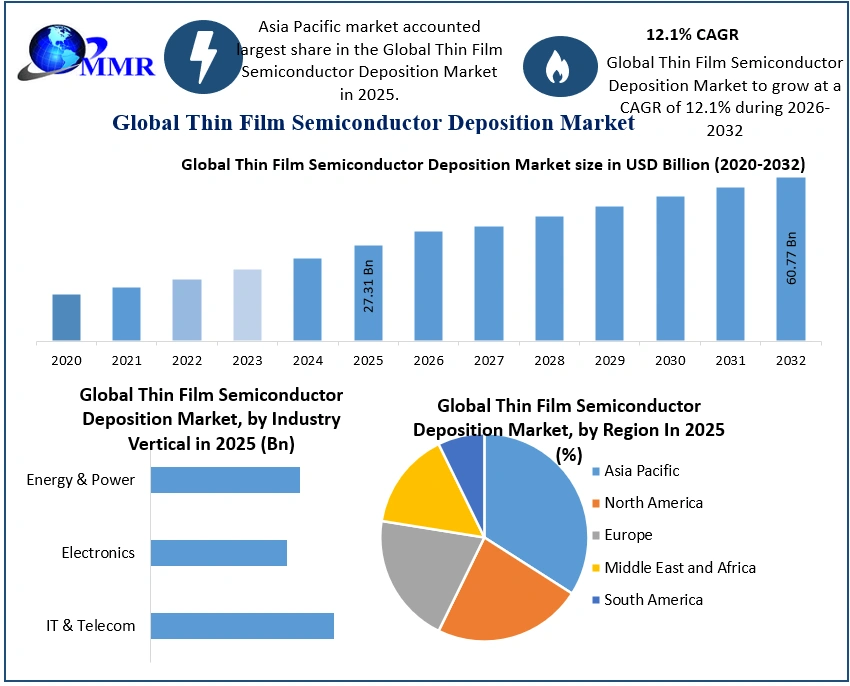
The Thin Film Semiconductor Deposition Market size was valued at USD 27.31 Billion in 2025 and the total Thin Film Semiconductor Deposition revenue is expected to grow at a CAGR of 12.1% from 2026 to 2032, reaching nearly USD 60.77 Billion by 2032.
Thin Film Semiconductor Deposition Market Dynamics:
The key factors driving the deposition market are impending need of circuit miniaturization, high investment by various governments in solar power plants, and technological developments in organic LED displays. However, high capital requirement for setting up a thin film fabrication facility is a major threat to the market growth.
To know about the Research Methodology:-Request Free Sample Report
The report study has analyzed revenue impact of covid-19 pandemic on the sales revenue of market leaders, market followers and disrupters in the report and same is reflected in our analysis.
In 2018, the CVD equipment market dominated the global thin film semiconductor deposition market with a 50.76% share in terms of profits. Maximize expects this segment to have the largest market share throughout the forecast period. The market is expected to grow at a CAGR of 13.33% to reach USD 49.30 billion in 2029 because of rising demand for semiconductor devices used in electronic products such as consumer electronics, industrial equipment, automotive, and healthcare equipment.
Among all deposition technology, CVD technology holds a significant revenue share in the world TFS deposition market, because of its low manufacturing cost, comparatively easier manufacturing process, and extensive use in fastest growing photovoltaic technology. In addition, CVD technology is expected to witness the fastest growth during the forecast period, with a CAGR of xx%. The growth would be driven by increase in demand of microelectronic components, electronic devices, and its expanding usage in sensors for smartphones which are growing rapidly across the globe.
Thin Film Semiconductor Deposition Market Segment Analysis
Based on Industry Vertical, the electronics segment has dominated the thin film semiconductor deposition market and is expected to maintain its lead during the forecast period. This is primarily due to the widespread use of thin film deposition in manufacturing integrated circuits, memory devices, displays, and sensors. The demand for compact, efficient, and high-performance electronic devices continues to rise with advancements in consumer electronics, automotive electronics, and IoT devices. Thin film deposition techniques enable precise layer formation at the nanoscale, ensuring reliability and efficiency, which makes the electronics segment the largest and most influential end-use sector driving market growth.
Based on Deposition Technology, the chemical vapor deposition (CVD) segment has dominated the thin film semiconductor deposition market and is expected to continue its lead during the forecast period. CVD is widely adopted because it provides high-quality, uniform, and durable thin films with excellent conformality, making it essential for integrated circuits, solar cells, and semiconductor devices. Its ability to handle large-scale production with high precision gives it a competitive edge over other techniques. With the increasing demand for miniaturized electronics and advanced photovoltaic solutions, the CVD segment will remain the most influential technology driving market growth.
Thin Film Semiconductor Deposition Market Regional Insights:
Asia-Pacific is the largest revenue-generating region in this market because of the presence of largest electronic equipment producers and consumers in the region followed by North America and Europe. Among the Asia-Pacific countries, China is the largest market with nearly 50% revenue share of the overall Asia-Pacific market because of heavy investment by the country in solar power and electronic giants setting up manufacturing facilities. Furthermore, the market in Asia-Pacific is expected to exhibit the highest growth, registering a CAGR of 14.9% during the forecast period.
Key players in the market have heavily invested in R&D activities to develop high-quality & high efficiency TFS to cater to the growth in demand of TFS across various applications. Further, TFS deposition market is fragmented, as top four leading players, Applied Materials, Tokyo Electron Limited, Lam Research, and Shin-Etsu Chemical Co., Ltd contribute around 40% of the overall market revenue. The key strategies adopted by these leading players are product launch, expansion, acquisition, partnership, and agreement to strengthen their market position and expand their geographical presence.
The objective of the report is to present a comprehensive assessment of the market and contains thoughtful insights, facts, historical data, industry-validated market data and projections with a suitable set of assumptions and methodology. The report also helps in understanding dynamics, structure by analyzing the market segments bydeposition technology, Industry Vertical and region and, project the global market size.
Report also provides a clear representation of competitive analysis of key players by product, price, financial position, product portfolio, growth strategies, and regional presence in the Deposition market. The report also provides PEST analysis, PORTER’s analysis, SWOT analysis to address the question of shareholders in arranging the efforts and investment in the near future to a particular market segment.
Key Highlights:
Global Deposition Market analysis and forecast, in terms of value.
Comprehensive study and analysis of market drivers, restraints and opportunities influencing the growth of the Global Thin Film Semiconductor Deposition Market
Global Deposition Market segmentation on the basis of type, source, end-user, and region (country-wise) has been provided.
The Deposition Market strategic analysis with respect to individual growth trends, future prospects along with the contribution of various sub-market stakeholders have been considered under the scope of study.
Global Deposition Market analysis and forecast for five major regions namely North America, Europe, Asia Pacific, the Middle East & Africa (MEA) and Latin America along with country-wise segmentation.
Profiles of key industry players, their strategic perspective, market positioning and analysis of core competencies are further profiled.
Competitive developments, investments, strategic expansion and competitive landscape of the key players operating in the Global Deposition Market are also profiled.
Scope of Global Thin Film Semiconductor Deposition Market: Inquire before buying
| Global Thin Film Semiconductor Deposition Market | |||
|---|---|---|---|
| Report Coverage | Details | ||
| Base Year: | 2025 | Forecast Period: | 2026-2032 |
| Historical Data: | 2020 to 2025 | Market Size in 2025: | USD 27.31 Bn. |
| Forecast Period 2026 to 2032 CAGR: | 12.1% | Market Size in 2032: | USD 60.77 Bn. |
| Segments Covered: | by Deposition Technology | Chemical Vapor Deposition (CVD) Physical Vapor Deposition (PVD) |
|
| by Industry Vertical | IT & Telecom Electronics Energy & Power |
||
| by Application | Solar Panels Microelectronics Data Storage Optical Coatings LEDs & OLED Displays Others |
||
Thin Film Semiconductor Deposition Market, by Region
North America (United States, Canada and Mexico)
Europe (UK, France, Germany, Italy, Spain, Sweden, Austria and Rest of Europe)
Asia Pacific (China, South Korea, Japan, India, Australia, Indonesia, Malaysia, Vietnam, Taiwan, Bangladesh, Pakistan and Rest of APAC)
Middle East and Africa (South Africa, GCC, Egypt, Nigeria and Rest of ME&A)
South America (Brazil, Argentina Rest of South America)
Thin Film Semiconductor Deposition Market, Key Players
1.Oerlikon Balzers
2.Hitachi Kokusai Electric Inc.
3.Tokyo Electron Limited
4.Applied Materials, Inc.
5.CVD Equipment Corporation
6.Lam Research Corporation
7.AIXTRON SE
8.Ihi Hauzer Techno Coating B.V
9.Sumco Corporation
10.Shin-Etsu Chemical Co., Ltd
11.Applied Materials
12.ULVAC
13.Kokusai Electric Inc.
14.Anwell Solar
15.Ascent Solar
Frequently Asked questions
1. What is the market size of the Global Thin Film Semiconductor Deposition Market in 2025?
Ans. The market size Global Deposition Market in 2025 was USD 27.31 Billion.
2. What are the different segments of the Global Thin Film Semiconductor Deposition Market?
Ans. The Global Deposition Market is divided into Deposition Technology and Industry Vertical and application.
3. What is the study period of this market?
Ans. The Global Deposition Market will be studied from 2025 to 2032.
4. Which region is expected to hold the highest Global Thin Film Semiconductor Deposition Market share?
Ans. The North America dominates the market share in the Thin Film Semiconductor Deposition market.
5. What is the Forecast Period of Global Thin Film Semiconductor Deposition Market?
Ans. The Forecast Period of the market is 2026-2032 in the market.