
Photolithography Market Size by Process, Application and Region – Segment-Level Market Assessment, Growth Opportunity Analysis, Competitive Mapping & Forecast to 2034
Overview
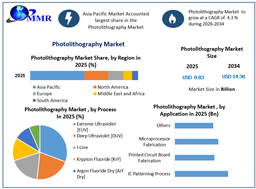
The Photolithography Market size was valued at USD 9.83 Billion in 2025 and the total Photolithography revenue is expected to grow at a CAGR of 4.3% from 2026 to 2034, reaching nearly USD 14.36 Billion.
Photolithography Market Overview:
Photolithography is the process of imprinting geometric patterns onto a substrate using optical radiations. It's also known as optical or ultraviolet (UV) lithography in some circumstances. Photolithography procedures include wafer cleaning, barrier layer production, photoresist application (including soft baking), mask alignment (including exposure and growth), and hard baking (also known as hard-baking). You'll need a very clear surface layer for etched designs, as well as ideal temperature settings, to succeed with this tough procedure. Integrated circuits (ICs), printed electronic boards, nameplates, and printing plates, to name a few, are all made possible by photolithographic technologies.
Photolithography Market Size, Growth & Share Analysis
To know about the Research Methodology :- Request Free Sample Report
Photolithography Market Dynamics:
Photolithography has the potential to become a critical application in a variety of industries, including healthcare, manufacturing, and aerospace and defence. Venture capitalists and government agencies are becoming interested in photolithography solutions.
The key drivers of the market's growth are the global increased of the consumer electronics industry and the introduction of advanced electronics items by global market participants. According to research, increased demand for photolithography in the manufacturing of printed circuit boards and microprocessors, increased production of computer chips, increased demand for photolithography in the integrated circuit (IC) industry, and a rapidly growing world electronics packaging market will all contribute to the market's growth during the forecast period. The advantages of photolithography technology include high sensitivity to light, outstanding adhesion properties, high resolution, and the capacity to 3D encapsulate cells inside hydrogels, all of which are propelling the market forward.
The high cost of machinery and the need for access to a clean room are two main stumbling blocks to the market's growth. A fast changing electronics industry could also limit market growth.
Photolithography Market Segment Analysis:
Based on the Process, the Photolithography market is sub-segmented into Extreme Ultraviolet [EUV], Deep Ultraviolet [DUV], I-Line, Krypton Fluoride [KrF], Argon Fluoride Dry [ArF Dry] and others. The Extreme Ultraviolet [EUV] segment held the largest market share of xx% in 2025. The demand for extreme UV method for production of electronics components grew as the semiconductor industry grew.
Manufacturing businesses should expose high-cost wafers on every wafer to create semiconductor devices. As a result, the EUV technique is advantageous to businesses since it exposes the crucial layer in a single step, lowering the cost of manufacturing semiconductor devices. The EUV technique employs a laser-produced plasma lighting source, lowering maintenance and operational costs. As a result, manufacturers are focusing on the extreme ultraviolet photolithography technique, which is driving the industry forward. Also, EUV-produced microprocessors are powerful, sophisticated, and very efficient.
Based on the Application, the Photolithography market is sub-segmented into IC Patterning Process, Printed Circuit Board Fabrication, Microprocessor Fabrication and Others. The IC Patterning Process segment held the largest market share of xx% in 2025. The surge is due to the increased use of photolithography in the integrated circuit industry around the world. An increase in demand for photolithography in semiconductor ICs for different applications such as communication devices, consumer electronic items, sensor devices, and memory devices is propelling the market forward.
Photolithography Market Regional Insights:
Asia Pacific held the largest market share of xx% in 2025 and it remain kept its leading position during the forecast period. The market is being propelled forward by emerging economies like as China, India, and Japan. The growing market for electronics and semiconductors in the region is responsible for the increase in the number of companies in the industry.
North America held the 2nd largest market share of xx% in 2025. The introduction of EUV lithography and comparable lithography processes in electronic device manufacture in this region has been aided by rapidly changing technology. Also, prominent technology providers in the region, such as Omega Optical and Applied Materials, have a beneficial impact on the size of the Photolithography market. In addition, the UV lithography market is driven by the growing demand for AI-based front-end and back-end applications, as well as advanced analytics platforms in the region.
The objective of the report is to present a comprehensive analysis of the global Photolithography Market to the stakeholders in the industry. The past and current status of the industry with the forecasted market size and trends are presented in the report with the analysis of complicated data in simple language. The report covers all the aspects of the industry with a dedicated study of key players that include market leaders, followers, and new entrants.
PORTER, PESTEL analysis with the potential impact of micro-economic factors of the market has been presented in the report. External as well as internal factors that are supposed to affect the business positively or negatively have been analyzed, which will give a clear futuristic view of the industry to the decision-makers.
The reports also helps in understanding the global Photolithography Market dynamic, structure by analyzing the market segments and project the global Photolithography Market size. Clear representation of competitive analysis of key players by product, price, financial position, product portfolio, growth strategies, and regional presence in the global Photolithography Market make the report investor’s guide.
Photolithography Market Recent Development
| Date | Company | Development | Impact |
|---|---|---|---|
| 06 May 2025 | TECHCET | Published a critical report forecasting a 7% revenue increase for photolithography materials in 2025 to reach $5.06 billion. | Highlights a robust market recovery driven by a 30% surge in demand for advanced EUV photoresists. |
| 02 September 2025 | ASML | Showcased its comprehensive holistic lithography portfolio at SEMICON India 2025 to support local chip manufacturing growth. | Aids emerging domestic fabs in achieving nanometer precision and cost-effective high-volume production for advanced nodes. |
| 15 July 2026 | ASML | Raised its full-year 2026 revenue guidance to €43–45 billion and announced plans to expand EUV lithography capacity by 30%. | Reflects strong, sustained equipment demand fueled by the global AI chipmaking boom and next-gen logic investments. |
| 16 July 2026 | ASML | Reported Q2 2026 total revenue of €9.33 billion, marking a 21% year-on-year increase driven by robust machine shipments. | Surpassed market consensus estimates and underscored accelerating capital deployment across major semiconductor fabrication plants. |
Photolithography Market Scope: Inquiry Before Buying
| Photolithography Market | |||
|---|---|---|---|
| Report Coverage | Details | ||
| Base Year: | 2025 | Forecast Period: | 2026-2034 |
| Historical Data: | 2020 to 2025 | Market Size in 2025: | USD 9.83 Bn. |
| Forecast Period 2026 to 2034 CAGR: | 4.3% | Market Size in 2034: | USD 14.36 Bn. |
| Segments Covered: | by Process | Extreme Ultraviolet [EUV] Deep Ultraviolet [DUV] I-Line Krypton Fluoride [KrF] Argon Fluoride Dry [ArF Dry] Others |
|
| by Application | IC Patterning Process Printed Circuit Board Fabrication Microprocessor Fabrication Others |
||
Photolithography Market, by Region
North America (United States, Canada and Mexico)
Europe (UK, France, Germany, Italy, Spain, Sweden, Austria and Rest of Europe)
Asia Pacific (China, South Korea, Japan, India, Australia, Indonesia, Malaysia, Vietnam, Taiwan, Bangladesh, Pakistan and Rest of APAC)
Middle East and Africa (South Africa, GCC, Egypt, Nigeria and Rest of ME&A)
South America (Brazil, Argentina Rest of South America)
Photolithography Market, Key Players are
1. ASML Holdings, N.V
2. Nikon Corporation
3. Canon, Inc
4. JEOL Ltd
5. NuFlare Technology
6. Ultratech, Inc
7. Rudolph Technologies, Inc
8. SUSS Mictotec, A.G
9. Nil Technology
10. EV Group
11. Carl Zeiss AG
12. Samsung Electronics
13. Tokyo Electron Limited
14. Applied Materials
15. Veeco Instruments Inc
16. Vistec Electron Beam GMBH
17. Shanghai Microelectronics equipment group
18. Taiwan Semiconductor Manufacturing Company Ltd
19. Advanced Micro Devices
20. Broadcom Limited
21. Hisilicon Technologies
22. Qualcomm
23. MediaTek
24. NXP Semiconductors
25. Xilinx
Frequently Asked Questions:
1] What segments are covered in Photolithography Market report?
Ans. The segments covered in Photolithography Market report are based on Process and Application.
2] Which region is expected to hold the highest share in the Photolithography Market?
Ans. Asia Pacific is expected to hold the highest share in the Photolithography Market.
3] What is the market size of Photolithography Market by 2034?
Ans. The market size of Photolithography Market is expected to reach USD 14.36 Bn. by 2034.
4] Who are the top key players in the Photolithography Market?
Ans. ASML Holdings, N.V, Nikon Corporation, Canon, Inc, JEOL Ltd, NuFlare Technology and Ultratech, Inc are the top key players in the global Photolithography Market.
5] What was the Global Photolithography Market size in 2025?
Ans: The Global Photolithography Market size was USD 9.83 Billion in 2025.