Thin Film Material Market by Deposition Process, Types, Applications and Region – Global Market Size Estimation, Industry-Wide Analysis, Competitive Landscape Assessment & Long-Term Forecast to 2032

4.2%
CAGR (2026-2032)
13.64 USD Bn.
Market Size
305
Report Pages
124
Market Tables

Overview

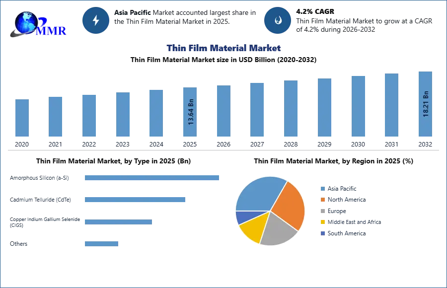
The Thin Film Material Market size was valued at USD 13.64 Billion in 2025 and the total Thin Film Material revenue is expected to grow at a CAGR of 4.2% from 2026 to 2032, reaching nearly USD 18.21 Billion.

Thin Film Material Market Overview:

Thin film materials are high-purity materials and chemicals utilized in the formation or modification of thin film deposits and substrates. Precursor gases, sputtering targets, and evaporation filaments are among the examples. A thin film is a layer of material that ranges in thickness from fractions of a nanometer (monolayer) to several micrometers. Thin film construction is mostly used in electronic semiconductor devices and optical coatings.

High demand from present and upcoming applications, growing desire for efficiency and miniaturization, technological innovation, government regulations, mandates, and subsidies are the drivers driving growth in the thin film material market. The poor conversion efficiency and large investments necessary in R&D and technology are factors restricting the growth of this industry.

Concerns about climate change and global warming have piqued the attention of numerous governments throughout the world in renewable and green energy sources. Countries such as Germany, India, the United States, and the United Kingdom are providing economic incentives and plans to stimulate and push the usage of renewable energy. Government subsidies have aided the growth of the solar power sector. Thin film materials, which are efficient, effective, and dependable, provide a solution to this challenge. One of the primary reasons for the MEMS industry's increased use of micro components is the ease with which these materials may be miniaturized.

Thin Film Material MarketTo know about the Research Methodology :- Request Free Sample Report

Thin Film Material Market Dynamics:

Rising demand for Thin Films across various industries

Thin films have been used in a variety of applications in recent years, including biosensors, wearable electronics, organic field-effect transistors, infrared or microbolometer detectors, and optoelectronic and electrochromic devices in the electronics industry; solar panels and transistors in the energy industry; wound healing devices in the biomedical industry, and primary or secondary packaging and engineered plastics in the food package industry. As a result, it is increasing global demand for Thin Film Materials.

Thin films quickly found industrial uses in ornamental and optical applications. The evolution of thin film technology, aided by the development of vacuum technology and electric power facilities, has increased the range of applications to the point where almost every industrial sector now utilizes them to provide specific physical and chemical properties to the surface of bulk materials. The ability to tailor the film properties by varying the microstructure via the deposition parameters used in a specific deposition technique has recently enabled their entry from the most basic applications such as protective coatings against wear and corrosion to the most technologically advanced applications such as microelectronics and biomedicine.


Growing awareness for Nanoparticles and Thin Films

Nanoparticles and thin films are currently among the most active materials science research domains for technological applications. The attraction in nanoscale systems derives not only from the goal of miniaturization, but also from the fact that novel characteristics emerge at this length scale, and that these properties fluctuate with size, surface-to-volume ratio, and form. Understanding and controlling nanoscale characteristics have enabled scientists and engineers to develop, theoretically model, manufacture, and describe materials as well as improved functional and multifunctional gadgets of current significance.

They would then continue to contribute many applications and a vast body of research, such as information technology, electronics, spintronics, displays, memory units, sensors, biosensors, actuators, active surfaces with various properties, catalysis, energy harvesting, energy storage, environmental and safety concerns, healthcare, bioengineering, medicine, the drug industry, and so on. The advancement of these systems of organic or inorganic nanomaterials has also resulted in the advancement of technical equipment and methodologies for their production and characterization, even down to the atomic and single molecular scale.


Rising demand for Thin Films in Microelectronics

Thin films, which may be made in a variety of ways, are used in a diverse range of microelectronic applications due to their adaptability, for example, transistors, sensors, memories, energy devices, and coatings. Additionally, the electronics sector has benefited the most from thin-film technology, which helps to advance microelectronics by shrinking the sizes of semiconductor devices.

These thin-film devices have excellent mechanical deformability, sensitivity to multifunctional responses, and intelligent control capabilities. This Special Issue includes fourteen papers that highlight materials synthesis, manufacturing procedures, and potential applications that address recent advances in microelectronic systems.

Thin films are utilized in semiconductor devices to generate the conducting lines that connect individual devices, as well as the contact pads to which wires connect the circuit to the encapsulating structure. They are also utilized to create insulating layers that separate conducting films from the underlying device structure.


High-quality optical thin films are relatively thick

The growth of laser technologies has significantly boosted the need for high-quality optical thin films with adjustable and well-defined physical features. Such coatings are commonly produced in thicknesses much shorter than visible light wavelengths, posing obstacles for characterization using standard microscopy. Due to their wide variety of refractive indices, optical absorption, and frequently near-complete reflectivity in the visible spectrum, metal films in particular highlight these challenges. The bulk optical characteristics of metal thin films, on the other hand, are mostly determined by their thickness due to their relatively uniform crystalline structure.

Thin Film Material Market Segment Analysis:

By Deposition Process, the Physical Vapor deposition (PVD) process segment held the largest market share in 2025 and is expected to dominate the market at the end of the forecast period. PVD Coating refers to a class of thin film deposition processes in which a solid material is vaporized in a vacuum atmosphere and deposited as a pure material or alloy composition coating on surfaces. It evaporates or sputters a substance, resulting in a gaseous plume or beam that deposits a coating on the substrate. It refers to a class of thin-film deposition processes that require vaporizing a solid material in a vacuum before depositing it on a substrate. These coatings are extremely robust and resistant to abrasion and corrosion.

PVD may be used to make everything from solar cells to eyewear to semiconductors. PVD has various advantages, including the development of a strong coating that is resistant to corrosion and scratches, which is driving segment growth over the forecast period. PVD can also produce thin coatings that can withstand high temperatures. Physical Vapor Deposition is the technology of choice for the surgical and medical implant industries due to its ability to produce very pure, clean, and durable coatings. Evaporation and magnetron sputtering are the most prevalent kinds of physical vapor deposition (PVD) and are commonly utilized by numerous end-user industries.

Cost is one of the potential drawbacks of PVD, since these technologies may demand a bigger investment than other thin film deposition procedures. The cost of PVD processes can also vary, which is a key restriction to segment growth.

Global Thin Film Material Market by Deposition Process

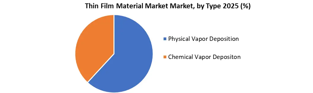
The Chemical Vapor Deposition (CVD) segment is expected to grow substantially during the forecast period. Chemical approaches include gas phase and liquid phase deposition. Chemical vapor deposition (CVD) and atomic layer epitaxy (ALE) are gas-phase procedures, whereas spray pyrolysis, sol-gel, and spin- and dip-coating are liquid-phase approaches. CVD utilizes reactive, volatile chemicals that disintegrate on a heated substrate. The starting ingredients are frequently oregano or hydrido-compounds, which pyrolyze at low temperatures into a nonvolatile (film) component and a pumpable vapor/gas component.

Both approaches are subdivided into several ways that use auxiliary processes to attain a certain purpose. The substrate is put in a vacuum chamber, and two chemical precursors are heated, causing them to evaporate. When they collide on the substrate surface, a chemical reaction ensues, resulting in the formation of a high-performance thin film coating.

Chemical vapor deposition's key qualities and distinctive properties include its ability to produce both simple and complicated chemicals with relative ease at typically low temperatures, good throwing power, and formation of a uniform thickness coating. CVD coating growth rate is high, with ease of epitaxial layer formation and strong repeatability of coating with same or nearly identical mechanical, optical, chemical, and physical characteristics. Additionally, CVD may deposit materials with low porosity that are difficult to evaporate on a substrate of intricate forms that are difficult to manufacture using conventional deposition processes.

CVD coatings are beneficial for a broad range of applications, including medical devices, automotive components, and silicon wafers. The capacity to cover complicated or complex topographies is one of the benefits of CVD procedures, as is the flexibility to apply these processes on a broad range of substrates. Thin films formed by CVD often retain their bonds effectively in high-stress settings.

Thin Film Material Market Regional Insights:

The Asia-Pacific region accounts for the largest market share in the thin film material market globally in 2025 and is expected to be the fastest-growing region over the forecast period. The region's growth is being driven by the increasing acceptance of technical breakthroughs, as well as increased industrial and assembly operations. Additionally, rising population, changing consumer lifestyles, rising solar photovoltaic cells for solar power production plants, rising demand for electronic products, and growing awareness of finite resources are expected to drive regional growth during the forecast period.

In terms of capacity, India and China control the majority of the largest solar photovoltaic power facilities. The Tengger solar park in China, located in Zhongwei, Ningxia, spans over 1,200 kilometers and generates 1,547 megawatts of power. The Bhadla solar farm in India, located in the Jodhpur area of Rajasthan, is scheduled to open in 2025. The plant's capacity is expected to be 2,255 megawatts of power and is distributed across 45 square kilometers. Innovative regional initiatives, such as the Thin-Film Solar Wall Project in Heyuan City, Guangdong Province, China, are expected to open up new doors for the market under consideration.

In addition, key businesses are utilizing methods such as new product releases and corporate expansions to strengthen their position in the global market. For example, Kaneka Corporation (Japan) announced the development of PixeoTM IB, a heat-resistant polyimide film, in November 2025. This new material introduction would allow the firm to increase its product portfolio and sales of 5G-supporting items, allowing digital gadgets to achieve improved functionality.

North America is seeing significant growth as a result of the region's sales output and industrial capacity. The easy availability of revolutionary technology, tight regulatory rules to reduce carbon emissions, and increased usage and deployment of solar panels are the primary drivers of the thin film industry's growth. Additionally, rising demand for thin film material from the IC manufacturing sectors is driving regional growth throughout the forecast period.

However, emerging industrial and electronic lines of business in developing economies such as the United Kingdom, Germany, France, Italy, and Spain are driving the European market. The rapid use of artificial illumination such as LEDs to boost crop performance, particularly in northern Europe, is driving the regional market growth. In addition, increased PV panel installation in Germany for greater energy independence would boost demand for thin films for PV material. Rooftop installations in the United States were increased by 20% in 2025, owing to lower solar technology prices, improved subsidy conditions, and other reasons.

The Middle East and Africa are anticipated to experience consistent growth as a result of hardware sector restructuring paired with growing development in the microelectronics industry, driving company growth. Latin America is facing significantly slower growth as a result of increased material production costs. Brazil is expected to be the most important market for thin film materials in Latin America during the forecast period, owing to increased demand for thin films in a variety of sectors.

Recent Industry Developments

Exact Date Company Development Impact
17 March 2026 Sono-Tek Corporation Entered a technical collaboration with Diamond Quanta to integrate precision ultrasonic coating for engineered diamond thin films on glass. This partnership advances thermal management and semiconductor performance by commercializing high-conductivity diamond-on-glass substrates.
11 March 2026 Sono-Tek Corporation Secured an $820,000 order for advanced thin-film coating systems specifically designed for diagnostic medical devices. Strengthens the company's market share in the high-growth medical coating segment, improving yield for bio-functional thin films.
14 January 2026 Samsung Display Announced the transition to Atomic Layer Deposition (ALD) for its 8.6-generation IT OLED lines to enhance thin-film encapsulation. This technological shift provides superior moisture barriers, significantly extending the lifespan of foldable and automotive display panels.
29 October 2025 First Solar, Inc. Commissioned a new R&D center focused on tandem perovskite-silicon thin-film modules to push commercial efficiency past 25%. Accelerates the commercialization of high-efficiency PV, reducing the levelized cost of energy (LCOE) for utility-scale solar projects.
13 October 2025 Sono-Tek Corporation Awarded a $2.8 million contract for the delivery of multiple ultrasonic deposition systems for next-generation electronics. Expands industrial capacity for functional thin films, meeting the surge in demand for miniaturized semiconductor components.
12 August 2025 Kaneka Corporation Launched a mass-production facility for flexible polyimide thin films optimized for high-speed 6G communication hardware. Positions the firm as a primary supplier for the next wave of ultra-high-frequency telecommunications and flexible circuit boards.

Thin Film Material Market Scope: Inquire before buying

Thin Film Material Market
Report Coverage Details
Base Year: 2025 Forecast Period: 2026-2032
Historical Data: 2020 to 2025 Market Size in 2025: 13.64 USD Billion
Forecast Period 2026-2032 CAGR: 4.2% Market Size in 2032: 18.21 USD Billion
Segments Covered: by Deposition Process Physical Vapor Deposition (PVD)
Chemical Vapor Deposition (CVD)
by Type Amorphous Silicon (a-Si)
Cadmium Telluride (CdTe)
Copper Indium Gallium Selenide (CIGS)
Others
by Application Photovoltaic Solar Cells
MEMS
Semiconductors & Electronics
Optical Coatings
Others
by End-User Video Surveillance
Traffic Monitoring
Security & Monitoring
Industrial Monitoring
Others

Thin Film Material Market, by Region

North America (United States, Canada and Mexico)
Europe (UK, France, Germany, Italy, Spain, Sweden, Austria, Turkey, Russia and Rest of Europe)
Asia Pacific (China, India, Japan, South Korea, Australia, ASEAN and Rest of APAC)
Middle East and Africa (South Africa, GCC, Egypt, Nigeria and Rest of ME&A)
South America (Brazil, Argentina, Columbia and Rest of South America)

Key Players / Competitors Profiles Covered in Brief in Global Thin Film Material Market Report in Strategic Perspective:

  1. Anwell Solar
  2. Ascent Solar Technologies Inc.
  3. Avancis GmbH
  4. Cicor Technologies Ltd.
  5. First Solar Inc.
  6. Hanergy Thin Film Power Group
  7. Kaneka Solar Energy
  8. Masdar PV GmbH
  9. Solar Frontier K.K.
  10. Suntech Power Holdings Co., Ltd.
  11. Trony Solar Holdings Co., Ltd.
  12. Moser Baer India Limited
  13. Stanford Advanced Materials
  14. Umicore Group
  15. JX Nippon Mining & Metals Corporation
  16. American Elements
  17. Corning Incorporated
  18. Global Solar Energy, Inc.
  19. MiaSolé Hi-Tech Corp.
  20. Solibro GmbH
  21. Oxford PV
  22. Samsung SDI Co., Ltd.
  23. Delta Optical Thin Film A/S
  24. China Singyes Solar Technologies Holdings Ltd.
  25. Kyocera Corporation

Table of Contents

1. Thin Film Material Market Introduction
1.1. Study Assumption and Market Definition
1.2. Scope of the Study
1.3. Executive Summary
2. Global Thin Film Material Market: Competitive Landscape
2.1. MMR Competition Matrix
2.2. Competitive Landscape
2.3. Key Players Benchmarking
2.3.1. Company Name
2.3.2. Business Segment
2.3.3. End-user Segment
2.3.4. Revenue (2025)
2.3.5. Company Locations
2.4. Leading Thin Film Material Market Companies, by market capitalization
2.5. Market Structure
2.5.1. Market Leaders
2.5.2. Market Followers
2.5.3. Emerging Players
2.6. Mergers and Acquisitions Details
3. Thin Film Material Market: Dynamics
3.1. Thin Film Material Market Trends by Region
3.1.1. North America Thin Film Material Market Trends
3.1.2. Europe Thin Film Material Market Trends
3.1.3. Asia Pacific Thin Film Material Market Trends
3.1.4. Middle East and Africa Thin Film Material Market Trends
3.1.5. South America Thin Film Material Market Trends
3.2. Thin Film Material Market Dynamics by Region
3.2.1. North America
3.2.1.1. North America Thin Film Material Market Drivers
3.2.1.2. North America Thin Film Material Market Restraints
3.2.1.3. North America Thin Film Material Market Opportunities
3.2.1.4. North America Thin Film Material Market Challenges
3.2.2. Europe
3.2.2.1. Europe Thin Film Material Market Drivers
3.2.2.2. Europe Thin Film Material Market Restraints
3.2.2.3. Europe Thin Film Material Market Opportunities
3.2.2.4. Europe Thin Film Material Market Challenges
3.2.3. Asia Pacific
3.2.3.1. Asia Pacific Thin Film Material Market Drivers
3.2.3.2. Asia Pacific Thin Film Material Market Restraints
3.2.3.3. Asia Pacific Thin Film Material Market Opportunities
3.2.3.4. Asia Pacific Thin Film Material Market Challenges
3.2.4. Middle East and Africa
3.2.4.1. Middle East and Africa Thin Film Material Market Drivers
3.2.4.2. Middle East and Africa Thin Film Material Market Restraints
3.2.4.3. Middle East and Africa Thin Film Material Market Opportunities
3.2.4.4. Middle East and Africa Thin Film Material Market Challenges
3.2.5. South America
3.2.5.1. South America Thin Film Material Market Drivers
3.2.5.2. South America Thin Film Material Market Restraints
3.2.5.3. South America Thin Film Material Market Opportunities
3.2.5.4. South America Thin Film Material Market Challenges
3.3. PORTER's Five Forces Analysis
3.4. PESTLE Analysis
3.5. Technology Roadmap
3.6. Regulatory Landscape by Region
3.6.1. North America
3.6.2. Europe
3.6.3. Asia Pacific
3.6.4. Middle East and Africa
3.6.5. South America
3.7. Key Opinion Leader Analysis For Thin Film Material Industry
3.8. Analysis of Government Schemes and Initiatives For Thin Film Material Industry
3.9. Thin Film Material Market Trade Analysis
3.10. The Global Pandemic Impact on Thin Film Material Market
4. Thin Film Material Market: Global Market Size and Forecast by Segmentation (in USD Billion) 2025-2032
4.1. Thin Film Material Market Size and Forecast, by Deposition Process (2025-2032)
4.1.1. Physical Vapor Deposition (PVD)
4.1.2. Chemical Vapor Deposition (CVD)
4.2. Thin Film Material Market Size and Forecast, by Type (2025-2032)
4.2.1. Amorphous Silicon (a-Si)
4.2.2. Cadmium Telluride (CdTe)
4.2.3. Copper Indium Gallium Selenide (CIGS)
4.2.4. Others
4.3. Thin Film Material Market Size and Forecast, by Application (2025-2032)
4.3.1. Photovoltaic Solar Cells
4.3.2. MEMS
4.3.3. Semiconductors & Electronics
4.3.4. Optical Coatings
4.3.5. Others
4.4. Thin Film Material Market Size and Forecast, by End-User (2025-2032)
4.4.1. Video Surveillance
4.4.2. Traffic Monitoring
4.4.3. Security & Monitoring
4.4.4. Industrial Monitoring
4.4.5. Others
4.5. Thin Film Material Market Size and Forecast, by Region (2025-2032)
4.5.1. North America
4.5.2. Europe
4.5.3. Asia Pacific
4.5.4. Middle East and Africa
4.5.5. South America
5. North America Thin Film Material Market Size and Forecast by Segmentation (in USD Billion) 2025-2032
5.1. North America Thin Film Material Market Size and Forecast, by Deposition Process (2025-2032)
5.1.1. Physical Vapor Deposition (PVD)
5.1.2. Chemical Vapor Deposition (CVD)
5.2. North America Thin Film Material Market Size and Forecast, by Type (2025-2032)
5.2.1. Amorphous Silicon (a-Si)
5.2.2. Cadmium Telluride (CdTe)
5.2.3. Copper Indium Gallium Selenide (CIGS)
5.2.4. Others
5.3. North America Thin Film Material Market Size and Forecast, by Application (2025-2032)
5.3.1. Photovoltaic Solar Cells
5.3.2. MEMS
5.3.3. Semiconductors & Electronics
5.3.4. Optical Coatings
5.3.5. Others
5.4. North America Thin Film Material Market Size and Forecast, by End-User (2025-2032)
5.4.1. Video Surveillance
5.4.2. Traffic Monitoring
5.4.3. Security & Monitoring
5.4.4. Industrial Monitoring
5.4.5. Others
5.5. North America Thin Film Material Market Size and Forecast, by Country (2025-2032)
5.5.1. United States
5.5.1.1. United States Thin Film Material Market Size and Forecast, by Deposition Process (2025-2032)
5.5.1.1.1. Physical Vapor Deposition (PVD)
5.5.1.1.2. Chemical Vapor Deposition (CVD)
5.5.1.2. United States Thin Film Material Market Size and Forecast, by Type (2025-2032)
5.5.1.2.1. Amorphous Silicon (a-Si)
5.5.1.2.2. Cadmium Telluride (CdTe)
5.5.1.2.3. Copper Indium Gallium Selenide (CIGS)
5.5.1.2.4. Others
5.5.1.3. United States Thin Film Material Market Size and Forecast, by Application (2025-2032)
5.5.1.3.1. Photovoltaic Solar Cells
5.5.1.3.2. MEMS
5.5.1.3.3. Semiconductors & Electronics
5.5.1.3.4. Optical Coatings
5.5.1.3.5. Others
5.5.1.4. United States Thin Film Material Market Size and Forecast, by End-User (2025-2032)
5.5.1.4.1. Video Surveillance
5.5.1.4.2. Traffic Monitoring
5.5.1.4.3. Security & Monitoring
5.5.1.4.4. Industrial Monitoring
5.5.1.4.5. Others
5.5.2. Canada
5.5.2.1. Canada Thin Film Material Market Size and Forecast, by Deposition Process (2025-2032)
5.5.2.1.1. Physical Vapor Deposition (PVD)
5.5.2.1.2. Chemical Vapor Deposition (CVD)
5.5.2.2. Canada Thin Film Material Market Size and Forecast, by Type (2025-2032)
5.5.2.2.1. Amorphous Silicon (a-Si)
5.5.2.2.2. Cadmium Telluride (CdTe)
5.5.2.2.3. Copper Indium Gallium Selenide (CIGS)
5.5.2.2.4. Others
5.5.2.3. Canada Thin Film Material Market Size and Forecast, by Application (2025-2032)
5.5.2.3.1. Photovoltaic Solar Cells
5.5.2.3.2. MEMS
5.5.2.3.3. Semiconductors & Electronics
5.5.2.3.4. Optical Coatings
5.5.2.3.5. Others
5.5.2.4. Canada Thin Film Material Market Size and Forecast, by End-User (2025-2032)
5.5.2.4.1. Video Surveillance
5.5.2.4.2. Traffic Monitoring
5.5.2.4.3. Security & Monitoring
5.5.2.4.4. Industrial Monitoring
5.5.2.4.5. Others
5.5.3. Mexico
5.5.3.1. Mexico Thin Film Material Market Size and Forecast, by Deposition Process (2025-2032)
5.5.3.1.1. Physical Vapor Deposition (PVD)
5.5.3.1.2. Chemical Vapor Deposition (CVD)
5.5.3.2. Mexico Thin Film Material Market Size and Forecast, by Type (2025-2032)
5.5.3.2.1. Amorphous Silicon (a-Si)
5.5.3.2.2. Cadmium Telluride (CdTe)
5.5.3.2.3. Copper Indium Gallium Selenide (CIGS)
5.5.3.2.4. Others
5.5.3.3. Mexico Thin Film Material Market Size and Forecast, by Application (2025-2032)
5.5.3.3.1. Photovoltaic Solar Cells
5.5.3.3.2. MEMS
5.5.3.3.3. Semiconductors & Electronics
5.5.3.3.4. Optical Coatings
5.5.3.3.5. Others
5.5.3.4. Mexico Thin Film Material Market Size and Forecast, by End-User (2025-2032)
5.5.3.4.1. Video Surveillance
5.5.3.4.2. Traffic Monitoring
5.5.3.4.3. Security & Monitoring
5.5.3.4.4. Industrial Monitoring
5.5.3.4.5. Others
6. Europe Thin Film Material Market Size and Forecast by Segmentation (in USD Billion) 2025-2032
6.1. Europe Thin Film Material Market Size and Forecast, by Deposition Process (2025-2032)
6.2. Europe Thin Film Material Market Size and Forecast, by Type (2025-2032)
6.3. Europe Thin Film Material Market Size and Forecast, by Application (2025-2032)
6.4. Europe Thin Film Material Market Size and Forecast, by End-User (2025-2032)
6.5. Europe Thin Film Material Market Size and Forecast, by Country (2025-2032)
6.5.1. United Kingdom
6.5.1.1. United Kingdom Thin Film Material Market Size and Forecast, by Deposition Process (2025-2032)
6.5.1.2. United Kingdom Thin Film Material Market Size and Forecast, by Type (2025-2032)
6.5.1.3. United Kingdom Thin Film Material Market Size and Forecast, by Application (2025-2032)
6.5.1.4. United Kingdom Thin Film Material Market Size and Forecast, by End-User (2025-2032)
6.5.2. France
6.5.2.1. France Thin Film Material Market Size and Forecast, by Deposition Process (2025-2032)
6.5.2.2. France Thin Film Material Market Size and Forecast, by Type (2025-2032)
6.5.2.3. France Thin Film Material Market Size and Forecast, by Application (2025-2032)
6.5.2.4. France Thin Film Material Market Size and Forecast, by End-User (2025-2032)
6.5.3. Germany
6.5.3.1. Germany Thin Film Material Market Size and Forecast, by Deposition Process (2025-2032)
6.5.3.2. Germany Thin Film Material Market Size and Forecast, by Type (2025-2032)
6.5.3.3. Germany Thin Film Material Market Size and Forecast, by Application (2025-2032)
6.5.3.4. Germany Thin Film Material Market Size and Forecast, by End-User (2025-2032)
6.5.4. Italy
6.5.4.1. Italy Thin Film Material Market Size and Forecast, by Deposition Process (2025-2032)
6.5.4.2. Italy Thin Film Material Market Size and Forecast, by Type (2025-2032)
6.5.4.3. Italy Thin Film Material Market Size and Forecast, by Application (2025-2032)
6.5.4.4. Italy Thin Film Material Market Size and Forecast, by End-User (2025-2032)
6.5.5. Spain
6.5.5.1. Spain Thin Film Material Market Size and Forecast, by Deposition Process (2025-2032)
6.5.5.2. Spain Thin Film Material Market Size and Forecast, by Type (2025-2032)
6.5.5.3. Spain Thin Film Material Market Size and Forecast, by Application (2025-2032)
6.5.5.4. Spain Thin Film Material Market Size and Forecast, by End-User (2025-2032)
6.5.6. Sweden
6.5.6.1. Sweden Thin Film Material Market Size and Forecast, by Deposition Process (2025-2032)
6.5.6.2. Sweden Thin Film Material Market Size and Forecast, by Type (2025-2032)
6.5.6.3. Sweden Thin Film Material Market Size and Forecast, by Application (2025-2032)
6.5.6.4. Sweden Thin Film Material Market Size and Forecast, by End-User (2025-2032)
6.5.7. Austria
6.5.7.1. Austria Thin Film Material Market Size and Forecast, by Deposition Process (2025-2032)
6.5.7.2. Austria Thin Film Material Market Size and Forecast, by Type (2025-2032)
6.5.7.3. Austria Thin Film Material Market Size and Forecast, by Application (2025-2032)
6.5.7.4. Austria Thin Film Material Market Size and Forecast, by End-User (2025-2032)
6.5.8. Rest of Europe
6.5.8.1. Rest of Europe Thin Film Material Market Size and Forecast, by Deposition Process (2025-2032)
6.5.8.2. Rest of Europe Thin Film Material Market Size and Forecast, by Type (2025-2032)
6.5.8.3. Rest of Europe Thin Film Material Market Size and Forecast, by Application (2025-2032)
6.5.8.4. Rest of Europe Thin Film Material Market Size and Forecast, by End-User (2025-2032)
7. Asia Pacific Thin Film Material Market Size and Forecast by Segmentation (in USD Billion) 2025-2032
7.1. Asia Pacific Thin Film Material Market Size and Forecast, by Deposition Process (2025-2032)
7.2. Asia Pacific Thin Film Material Market Size and Forecast, by Type (2025-2032)
7.3. Asia Pacific Thin Film Material Market Size and Forecast, by Application (2025-2032)
7.4. Asia Pacific Thin Film Material Market Size and Forecast, by End-User (2025-2032)
7.5. Asia Pacific Thin Film Material Market Size and Forecast, by Country (2025-2032)
7.5.1. China
7.5.1.1. China Thin Film Material Market Size and Forecast, by Deposition Process (2025-2032)
7.5.1.2. China Thin Film Material Market Size and Forecast, by Type (2025-2032)
7.5.1.3. China Thin Film Material Market Size and Forecast, by Application (2025-2032)
7.5.1.4. China Thin Film Material Market Size and Forecast, by End-User (2025-2032)
7.5.2. S Korea
7.5.2.1. S Korea Thin Film Material Market Size and Forecast, by Deposition Process (2025-2032)
7.5.2.2. S Korea Thin Film Material Market Size and Forecast, by Type (2025-2032)
7.5.2.3. S Korea Thin Film Material Market Size and Forecast, by Application (2025-2032)
7.5.2.4. S Korea Thin Film Material Market Size and Forecast, by End-User (2025-2032)
7.5.3. Japan
7.5.3.1. Japan Thin Film Material Market Size and Forecast, by Deposition Process (2025-2032)
7.5.3.2. Japan Thin Film Material Market Size and Forecast, by Type (2025-2032)
7.5.3.3. Japan Thin Film Material Market Size and Forecast, by Application (2025-2032)
7.5.3.4. Japan Thin Film Material Market Size and Forecast, by End-User (2025-2032)
7.5.4. India
7.5.4.1. India Thin Film Material Market Size and Forecast, by Deposition Process (2025-2032)
7.5.4.2. India Thin Film Material Market Size and Forecast, by Type (2025-2032)
7.5.4.3. India Thin Film Material Market Size and Forecast, by Application (2025-2032)
7.5.4.4. India Thin Film Material Market Size and Forecast, by End-User (2025-2032)
7.5.5. Australia
7.5.5.1. Australia Thin Film Material Market Size and Forecast, by Deposition Process (2025-2032)
7.5.5.2. Australia Thin Film Material Market Size and Forecast, by Type (2025-2032)
7.5.5.3. Australia Thin Film Material Market Size and Forecast, by Application (2025-2032)
7.5.5.4. Australia Thin Film Material Market Size and Forecast, by End-User (2025-2032)
7.5.6. Indonesia
7.5.6.1. Indonesia Thin Film Material Market Size and Forecast, by Deposition Process (2025-2032)
7.5.6.2. Indonesia Thin Film Material Market Size and Forecast, by Type (2025-2032)
7.5.6.3. Indonesia Thin Film Material Market Size and Forecast, by Application (2025-2032)
7.5.6.4. Indonesia Thin Film Material Market Size and Forecast, by End-User (2025-2032)
7.5.7. Malaysia
7.5.7.1. Malaysia Thin Film Material Market Size and Forecast, by Deposition Process (2025-2032)
7.5.7.2. Malaysia Thin Film Material Market Size and Forecast, by Type (2025-2032)
7.5.7.3. Malaysia Thin Film Material Market Size and Forecast, by Application (2025-2032)
7.5.7.4. Malaysia Thin Film Material Market Size and Forecast, by End-User (2025-2032)
7.5.8. Vietnam
7.5.8.1. Vietnam Thin Film Material Market Size and Forecast, by Deposition Process (2025-2032)
7.5.8.2. Vietnam Thin Film Material Market Size and Forecast, by Type (2025-2032)
7.5.8.3. Vietnam Thin Film Material Market Size and Forecast, by Application (2025-2032)
7.5.8.4. Vietnam Thin Film Material Market Size and Forecast, by End-User (2025-2032)
7.5.9. Taiwan
7.5.9.1. Taiwan Thin Film Material Market Size and Forecast, by Deposition Process (2025-2032)
7.5.9.2. Taiwan Thin Film Material Market Size and Forecast, by Type (2025-2032)
7.5.9.3. Taiwan Thin Film Material Market Size and Forecast, by Application (2025-2032)
7.5.9.4. Taiwan Thin Film Material Market Size and Forecast, by End-User (2025-2032)
7.5.10. Rest of Asia Pacific
7.5.10.1. Rest of Asia Pacific Thin Film Material Market Size and Forecast, by Deposition Process (2025-2032)
7.5.10.2. Rest of Asia Pacific Thin Film Material Market Size and Forecast, by Type (2025-2032)
7.5.10.3. Rest of Asia Pacific Thin Film Material Market Size and Forecast, by Application (2025-2032)
7.5.10.4. Rest of Asia Pacific Thin Film Material Market Size and Forecast, by End-User (2025-2032)
8. Middle East and Africa Thin Film Material Market Size and Forecast by Segmentation (in USD Billion) 2025-2032
8.1. Middle East and Africa Thin Film Material Market Size and Forecast, by Deposition Process (2025-2032)
8.2. Middle East and Africa Thin Film Material Market Size and Forecast, by Type (2025-2032)
8.3. Middle East and Africa Thin Film Material Market Size and Forecast, by Application (2025-2032)
8.4. Middle East and Africa Thin Film Material Market Size and Forecast, by End-User (2025-2032)
8.5. Middle East and Africa Thin Film Material Market Size and Forecast, by Country (2025-2032)
8.5.1. South Africa
8.5.1.1. South Africa Thin Film Material Market Size and Forecast, by Deposition Process (2025-2032)
8.5.1.2. South Africa Thin Film Material Market Size and Forecast, by Type (2025-2032)
8.5.1.3. South Africa Thin Film Material Market Size and Forecast, by Application (2025-2032)
8.5.1.4. South Africa Thin Film Material Market Size and Forecast, by End-User (2025-2032)
8.5.2. GCC
8.5.2.1. GCC Thin Film Material Market Size and Forecast, by Deposition Process (2025-2032)
8.5.2.2. GCC Thin Film Material Market Size and Forecast, by Type (2025-2032)
8.5.2.3. GCC Thin Film Material Market Size and Forecast, by Application (2025-2032)
8.5.2.4. GCC Thin Film Material Market Size and Forecast, by End-User (2025-2032)
8.5.3. Nigeria
8.5.3.1. Nigeria Thin Film Material Market Size and Forecast, by Deposition Process (2025-2032)
8.5.3.2. Nigeria Thin Film Material Market Size and Forecast, by Type (2025-2032)
8.5.3.3. Nigeria Thin Film Material Market Size and Forecast, by Application (2025-2032)
8.5.3.4. Nigeria Thin Film Material Market Size and Forecast, by End-User (2025-2032)
8.5.4. Rest of ME&A
8.5.4.1. Rest of ME&A Thin Film Material Market Size and Forecast, by Deposition Process (2025-2032)
8.5.4.2. Rest of ME&A Thin Film Material Market Size and Forecast, by Type (2025-2032)
8.5.4.3. Rest of ME&A Thin Film Material Market Size and Forecast, by Application (2025-2032)
8.5.4.4. Rest of ME&A Thin Film Material Market Size and Forecast, by End-User (2025-2032)
9. South America Thin Film Material Market Size and Forecast by Segmentation (in USD Billion) 2025-2032
9.1. South America Thin Film Material Market Size and Forecast, by Deposition Process (2025-2032)
9.2. South America Thin Film Material Market Size and Forecast, by Type (2025-2032)
9.3. South America Thin Film Material Market Size and Forecast, by Application (2025-2032)
9.4. South America Thin Film Material Market Size and Forecast, by End-User (2025-2032)
9.5. South America Thin Film Material Market Size and Forecast, by Country (2025-2032)
9.5.1. Brazil
9.5.1.1. Brazil Thin Film Material Market Size and Forecast, by Deposition Process (2025-2032)
9.5.1.2. Brazil Thin Film Material Market Size and Forecast, by Type (2025-2032)
9.5.1.3. Brazil Thin Film Material Market Size and Forecast, by Application (2025-2032)
9.5.1.4. Brazil Thin Film Material Market Size and Forecast, by End-User (2025-2032)
9.5.2. Argentina
9.5.2.1. Argentina Thin Film Material Market Size and Forecast, by Deposition Process (2025-2032)
9.5.2.2. Argentina Thin Film Material Market Size and Forecast, by Type (2025-2032)
9.5.2.3. Argentina Thin Film Material Market Size and Forecast, by Application (2025-2032)
9.5.2.4. Argentina Thin Film Material Market Size and Forecast, by End-User (2025-2032)
9.5.3. Rest Of South America
9.5.3.1. Rest Of South America Thin Film Material Market Size and Forecast, by Deposition Process (2025-2032)
9.5.3.2. Rest Of South America Thin Film Material Market Size and Forecast, by Type (2025-2032)
9.5.3.3. Rest Of South America Thin Film Material Market Size and Forecast, by Application (2025-2032)
9.5.3.4. Rest Of South America Thin Film Material Market Size and Forecast, by End-User (2025-2032)
10. Company Profile: Key Players
10.1. Anwell Solar
10.1.1. Company Overview
10.1.2. Business Portfolio
10.1.3. Financial Overview
10.1.4. SWOT Analysis
10.1.5. Strategic Analysis
10.1.6. Scale of Operation (small, medium, and large)
10.1.7. Details on Partnership
10.1.8. Regulatory Accreditations and Certifications Received by Them
10.1.9. Awards Received by the Firm
10.1.10. Recent Developments
10.2. Ascent Solar Technologies Inc.
10.3. Avancis GmbH
10.4. Cicor Technologies Ltd.
10.5. First Solar Inc.
10.6. Hanergy Thin Film Power Group
10.7. Kaneka Solar Energy
10.8. Masdar PV GmbH
10.9. Solar Frontier K.K.
10.10. Suntech Power Holdings Co. Ltd.
10.11. Trony Solar Holdings Co. Ltd.
10.12. Moser Baer India Limited
10.13. Stanford Advanced Materials
10.14. Umicore Group
10.15. JX Nippon Mining & Metals Corporation
10.16. American Elements
10.17. Corning Incorporated
10.18. Global Solar Energy Inc.
10.19. MiaSolé Hi-Tech Corp.
10.20. Solibro GmbH
10.21. Oxford PV
10.22. Samsung SDI Co. Ltd.
10.23. Delta Optical Thin Film A/S
10.24. China Singyes Solar Technologies Holdings Ltd.
10.25. Kyocera Corporation
11. Key Findings
12. Industry Recommendations
13. Thin Film Material Market: Research Methodology
14. Terms and Glossary

Custom Market Research Services

We Will Customise The Research For You, In Case The Report Listed Above Does Not Meet With Your Requirements