
Glass Wafer Carrier Market By Material Type, By Product Configuration, By Surface Configuration, By Wafer Diameter, By Thickness, By Application, By Workpiece Type, By End User, By Sales Channel and Regional Insights 2034
Overview
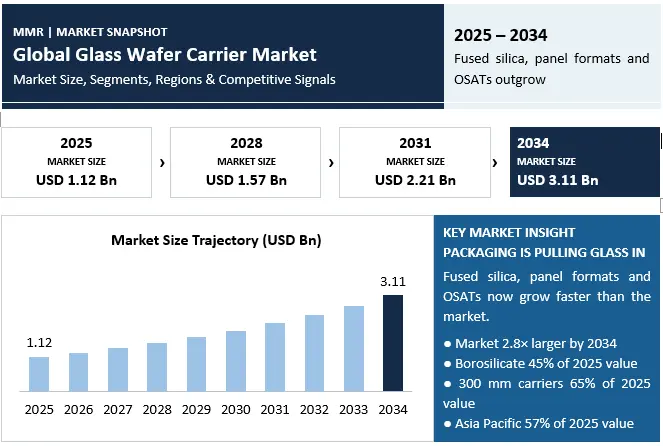
The Global Glass Wafer Carrier Market was valued at USD 1.12 billion in 2025 and is projected to reach USD 3.11 billion by 2034, growing at a CAGR of 12.0% during 2026–2034, according to Maximize Market Research (MMR). A glass wafer carrier is a precision-engineered glass plate that temporarily supports a semiconductor wafer or reconstituted panel while it is thinned, patterned and packaged, and is then released by thermal, UV or laser debonding. Because glass is flat, rigid and transparent, it has become a core consumable in advanced packaging.
This glass wafer carrier market analysis answers both sides of the search: what the market is worth for glass makers, wafer processors and investors, and what process engineers want to know, from how a temporary glass wafer carrier works in temporary wafer bonding and debonding to the choice of glass carrier substrate, the role of the semiconductor glass carrier in wafer thinning, and the specifications used in 3D IC and fan-out packaging.
Borosilicate glass and 300 mm carriers anchor the market, and foundries, integrated device manufacturers (IDMs) and outsourced semiconductor assembly and test providers (OSATs) are the largest buyers, but glass wafer carrier market growth is shifting toward fused silica, panel-level formats, release-layer-coated carriers and OSATs as AI accelerators, high-bandwidth memory and chiplet designs push packaging toward thinner wafers and larger panels.
Maximize Market Research provides comprehensive analysis of global glass wafer carrier market size, share, material type, product configuration, surface configuration, wafer diameter, thickness, application, workpiece type, end user, sales channel and regional segmentation, the glass wafer carrier manufacturers landscape, strategic scenarios and growth opportunities. The report helps glass manufacturers, precision wafer processors, bonding and debonding material suppliers, equipment makers, foundries, OSATs and investors decide which segments, channels and countries to prioritise through 2034.
| 2025 | BASE YEAR | 2034 | FORECAST | GROWTH RATE | LARGEST REGION |
| USD 1.12 Bn | USD 3.11 Bn | 12.0% | Asia Pacific |
Global Glass Wafer Carrier Market Overview:
The market is measured at product level across glass carrier wafers and panels used as temporary supports in semiconductor manufacturing, covering borosilicate, aluminosilicate, fused silica, quartz and other specialty glass carriers in bare, release-layer-coated and functionally coated forms. Permanent glass core substrates, glass interposers and display glass are treated as adjacent technologies and are excluded from market value, as are silicon carriers.
Three shifts shape 2026–2034: demand is broadening from wafer thinning into fan-out and 2.5D/3D packaging; value is moving toward fused silica, large-format and release-layer-coated carriers; and the 300 mm class is being joined by panel-level formats. Glass wafer carrier manufacturers are answering with ultra-low total thickness variation (TTV), low-CTE compositions and laser-compatible surfaces.
Global Glass Wafer Carrier Market Size, Growth & Share Analysis
To know about the Research Methodology :- Request Free Sample Report
Glass Wafer Carrier Quick Answers: 20 Most-Searched Questions About Glass Wafer Carriers, Answered in One Line
This report is built around what process engineers, packaging managers, glass manufacturers and investors actually search for. Use this table for instant answers, then jump to the section named in the last column.
Key Findings: Eight Insights Shaping the Global Glass Wafer Carrier Market
MMR’s analysis of published market data, company filings, industry announcements and technical literature points to eight findings that explain where glass wafer carrier market growth and value are created through 2034.
| Sr.No. | Findings | Evidence | So what |
| 1 | The market nearly triples by 2034 | USD 1.12 Bn (2025) to USD 3.11 Bn (2034) at 12.0% CAGR | Glass capacity, polishing yield and metrology must scale about 2.8× by 2034 |
| 2 | Borosilicate is the base, fused silica the growth edge | Borosilicate 45% of 2025 value; fused silica 14.5% CAGR | UV-transparent premium grades lift mix and margin |
| 3 | Asia Pacific is the largest region | 57% share in 2025, led by Taiwan, South Korea, China and Japan | Fab and OSAT clusters set qualification standards and pricing |
| 4 | North America is the fastest-growing region | 13.4% CAGR on CHIPS Act-backed packaging and glass-substrate projects | Locally qualified supply can win reshored volume |
| 5 | Fan-out packaging anchors demand | Fan-out wafer-level 37% of 2025 value; wafer thinning 28% | Flatness, TTV and reuse cycles decide supplier retention |
| 6 | Panel-level carriers outgrow wafers | Fan-out panel-level 16.0% CAGR; carriers above 300 mm 17% | Large-format capability becomes the differentiator |
| 7 | Silicon carriers and breakage are the main threats | Silicon carriers substitute in cost-led lines; large glass panels break more often than silicon | Edge strength, strengthening and reclaim services protect share |
| 8 | OSATs gain share | OSATs 24% of 2025 value and 13.6% CAGR as packaging is outsourced | Qualification with OSATs and foundries wins long-term contracts |
Global Glass Wafer Carrier Market Size, Share and Forecast, 2025–2034
MMR sizes the Global Glass Wafer Carrier Market at USD 1.12 billion in 2025, rising to USD 1.25 billion in 2026 and USD 3.11 billion in 2034, a 12.0% CAGR. The glass wafer carrier market forecast adds about USD 1.99 billion over the period; about 64% of the 2034 market is revenue that does not exist today. Published estimates differ because of scope and base year: 2025 values range from about USD 0.74 billion to USD 1.85 billion and growth rates from about 5% to 18%, depending on whether panel-level carriers, coated carriers and reclaim are counted. MMR’s base includes all of them.
Global Glass Wafer Carrier Market Dynamics:
Global Glass Wafer Carrier Market Growth Drivers: Advanced Packaging, Fan-Out, Thin-Wafer Processing and 3D IC Stacking
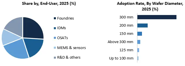
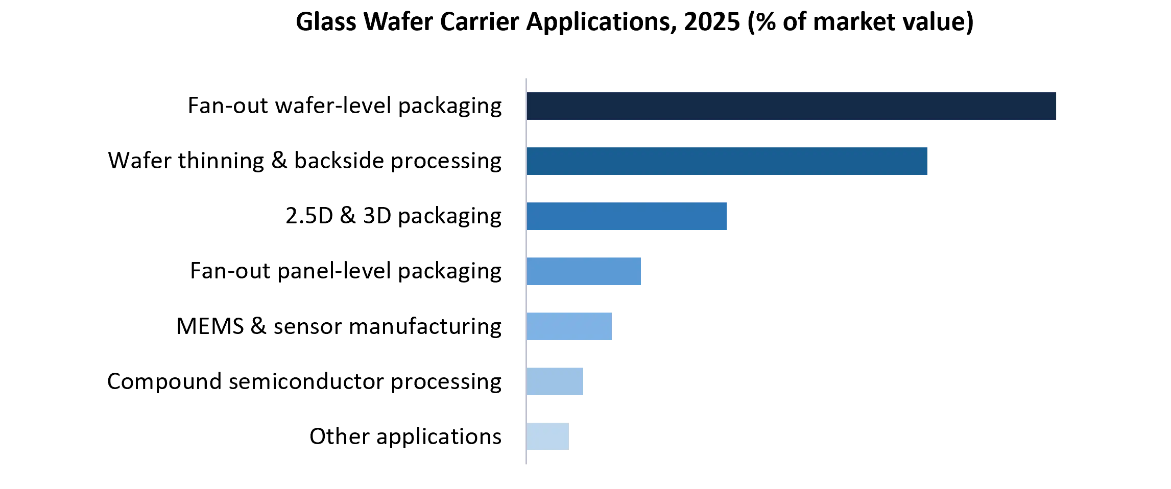
The Global Glass Wafer Carrier Market is supported by the shift of semiconductor value from transistor scaling to advanced packaging. A glass wafer carrier for semiconductor manufacturing gives thin device wafers the rigidity, flatness and thermal stability they need during backgrinding, through-silicon via (TSV) formation, redistribution layer (RDL) build-up and backside metallisation. Fan-out wafer-level packaging is the largest application at about 37% of 2025 value, and a glass carrier for fan-out wafer-level packaging holds reconstituted wafers flat while fine-pitch copper lines are built, a task that organic supports handle less well as dies are thinned to tens of microns. The glass carrier for wafer thinning accounts for about 28% of value, and the glass wafer carrier for 3D IC packaging, used for TSV, stacking and hybrid bonding, supplies roughly 14%. Because carriers are bonded, processed, debonded, cleaned and in many cases reused, demand is recurring rather than one-off, and 300 mm carriers, at about 65% of 2025 value, track the build-out of 300 mm fabs and packaging lines across Taiwan, South Korea, China and the United States.
Material and process changes are adding new layers of demand. Temporary wafer bonding with laser or UV release needs transparent carriers, which favours fused silica and low-CTE aluminosilicate and lifts demand for release-layer-coated carriers, about 33% of 2025 value and growing at 13.8% CAGR. Panel-level packaging for AI accelerators is moving toward large glass panels: Samsung announced a USD 2.3 billion alliance with glass-substrate partners in January 2025 to reach 650 × 650 mm mass production by 2026, and PLANOPTIK has upgraded a facility in Hungary for 650 mm plate capability. Government support adds further pull, as the US CHIPS Act has allocated about USD 52 billion to semiconductor reshoring, including up to USD 75 million for Absolics’ glass-substrate plant. Published industry data also show high-bandwidth memory output rising about 67% in 2024 as memory makers moved beyond 16-layer stacks, which raises the number of ultra-thin wafers that need support.
Global Glass Wafer Carrier Market Restraints: Precision-Glass Cost, Breakage, Silicon Substitution and Feedstock SupplyHigh cost and capital intensity are the main restraints. Precision glass is priced about three to five times above silicon equivalents, and ultra-flat grinding, double-side polishing and interferometric metrology equipment can take up to 70% of a greenfield plant’s capital budget, according to published industry analysis. Brittleness is a second constraint: large-panel carriers fracture at rates near 4%, against under 0.1% for silicon, and edge chips during automated transport and thermal cycling reduce yields and raise replacement demand. Margins are also exposed to inventory corrections and competitive quotes, as PLANOPTIK’s 2024 revenue compression showed.
Substitution, supply and qualification also limit growth. Silicon carriers combined with infrared nanocleaving offer a lower-cost route for some entry-level flows, particularly in North America and Europe, and could cannibalise standard glass volumes if adoption widens. Float-glass feedstock can be constrained when solar-PV lines draw on the same capacity, and energy costs and currency movements affect specialty glass producers’ economics. Customers qualify carriers process by process, so adoption can take many months, and suppliers must meet SEMI wafer-geometry specifications, ISO 9001 and ISO 14001 requirements and cleanroom contamination-control rules, which adds time and cost for new entrants.
What Are the Biggest Glass Wafer Carrier Market Opportunities Through 2034?
Fused silica, panel-level formats and release-layer-coated carriers represent the most significant opportunities because they lift value per carrier. Fused silica is projected to grow at 14.5% CAGR as laser and photonic debonding, high-temperature memory flows and UV transparency favour it, while fan-out panel-level packaging is projected at 16.0% CAGR and carriers above 300 mm at about 17%. Coated carriers that integrate light-to-heat conversion layers, and carriers with improved UV transmittance, let suppliers sell a validated process component rather than a plain plate. Reclaim and reuse services, which polish and recoat carriers after several cycles, can lower the customer’s total cost of ownership and lengthen supplier relationships.
Customisation, regional capacity and adjacent glass platforms offer further routes to growth. North America is projected to be the fastest-growing region at 13.4% CAGR as CHIPS Act-backed projects and glass-substrate pilots localise supply, while Europe benefits from automotive, MEMS and sensor demand. Custom-engineered and structured carriers, with cavities or engineered surface features, serve MEMS, RF and compound-semiconductor lines, where silicon carbide and gallium nitride wafers need specialised support. Glass interposers, through-glass vias and glass core substrates are separate products, but they bring glass-processing capacity, metrology and customer relationships that carrier suppliers can extend into, and OSATs, growing at 13.6% CAGR, are the buyers most open to new qualification.
Glass Wafer Carrier Market Trends: Large-Format Panels, Ultra-Low TTV, Laser Debonding and Reusable Carriers
Four glass wafer carrier market trends stand out through 2034. First, large formats: suppliers and packaging houses are moving from 300 mm wafers toward 510 × 515 mm and 650 × 650 mm panels, as seen in AGC’s advanced-packaging glass panels and Samsung’s alliance. Second, ultra-low TTV and flatness: ultra-flat carriers, about 27% of 2025 value, are gaining share as thinner wafers tolerate less variation, with ground flatness of 0.1 µm cited for Nippon Electric Glass’s GC Core glass. Third, laser-assisted debonding: transparent carriers with light-to-heat conversion layers cut debond time and avoid heat-induced warpage, supported by equipment such as LPKF’s Vitrion platform, expanded in January 2025. Fourth, reuse and reclaim: carriers pass through repeated bond, debond and clean cycles, so reclaim qualification and traceability become purchase criteria alongside price.
Global Glass Wafer Carrier Market Segment Analysis:
Glass Wafer Carrier Market by End User and Wafer Diameter: Foundries, IDMs, OSATs and 300 mm Carriers
Glass Carrier Substrate Market by Material, Product Configuration, Surface Configuration and Sales Channel Analysis
Borosilicate glass carriers are the largest material type at about 45% of 2025 value, valued for thermal expansion close to silicon and lower cost, while fused silica holds about 22%, aluminosilicate about 16%, quartz about 10% and other specialty glasses about 7%. Fused silica is the fastest-growing material at 14.5% CAGR. By product configuration, standard flat carriers lead at about 38% of 2025 value, followed by ultra-flat carriers at 27%, structured carriers at 14%, custom-engineered carriers at 13% and cavity-structured carriers at 8%. Bare glass carriers account for about 55% of value, release-layer-coated carriers about 33% and functional film-coated carriers about 12%. By thickness, standard-thickness carriers hold about 60%, thick carriers 22% and ultra-thin carriers 18%. Direct manufacturer sales remain the largest channel at about 58%, while online and industrial procurement platforms are the fastest at about 13.6% CAGR.
| Segmentation | Largest segment (2025 share) | Fastest segment (CAGR) | MMR view |
| Material type | Borosilicate glass carriers (45%) | Fused silica glass carriers (14.5%) | Defend borosilicate cost position, scale fused silica |
| Product configuration | Standard flat glass carriers (38%) | Ultra-flat glass carriers (15.5%) | Flatness and TTV drive upgrades |
| Surface configuration | Bare glass carriers (55%) | Release-layer-coated carriers (13.8%) | Coatings turn a plate into a process component |
| Wafer diameter | 300 mm carriers (65%) | Above 300 mm carriers (17.0%) | Panels extend carriers beyond wafers |
| Thickness | Standard-thickness carriers (60%) | Ultra-thin carriers (14.8%) | Thinner wafers need thin, stable carriers |
| Application | Fan-out wafer-level packaging (37%) | Fan-out panel-level packaging (16.0%) | Wafer-level anchors; panels add growth |
| Workpiece type | Silicon device wafers (58%) | Reconstituted wafers and panels (15.2%) | Reconstituted formats outgrow silicon wafers |
| End user | Semiconductor foundries (26%) | OSATs (13.6%) | OSAT qualification decides new share |
| Sales channel | Direct manufacturer sales (58%) | Online and industrial procurement (13.6%) | Direct for qualified programmes, online for standard items |
Glass Wafer Carrier Applications: Where Glass Wafer Carrier Demand Sits
Global Glass Wafer Carrier Market Regional Analysis:
Asia Pacific is the largest regional market, accounting for about 57% of global value in 2025. Taiwan, South Korea, China and Japan host the leading foundries, memory makers, OSATs and specialty glass producers, and local supply chains for float glass, grinding and polishing shorten qualification and freight. Japan supports the region through Nippon Electric Glass, AGC, HOYA and OHARA, Chinese precision-glass suppliers are expanding carrier capacity, and Singapore and Malaysia add packaging and test demand. Asia Pacific is projected to grow at about 11.8% CAGR through 2034. North America holds about 21% of 2025 value and is projected to be the fastest-growing region at about 13.4% CAGR, supported by CHIPS Act funding, Corning’s pilot of UV-transparent carriers, Absolics’ glass-substrate plant and Intel’s glass-substrate programme, while Canada and Mexico add smaller packaging and research demand.
Europe holds about 17% of 2025 value and is expected to grow at about 11.0% CAGR, anchored by SCHOTT in Germany, PLANOPTIK, LPKF, SUSS MicroTec, EV Group and SILEX Microsystems, and by demand from automotive, industrial electronics, MEMS and sensor makers. SCHOTT budgeted USD 150 million for precision glass tools in Germany and Singapore in December 2024, and PLANOPTIK’s Hungarian upgrade adds 650 mm plate capability. Middle East & Africa is a small market, about 3% of 2025 value, growing at about 12.5% CAGR from a low base as Israel, the United Arab Emirates and Saudi Arabia invest in semiconductor and electronics manufacturing. South America, about 2% of 2025 value, is projected to grow at about 10.0% CAGR, led by Brazil, where packaging and testing activity is developing but depends on imported carriers and distributors.
Glass Wafer Carrier Manufacturers and Competitive Landscape:
The glass wafer carrier competitive landscape includes several distinct groups rather than a single set of comparable companies. Multi-industry specialty glass leaders such as Corning, SCHOTT, AGC, Nippon Electric Glass, HOYA and OHARA melt and form the glass and supply carrier wafers and panels at global scale. Precision wafer processors and carrier fabricators, including PLANOPTIK, TECNISCO, Swift Glass, Sydor Optics, Coresix Precision Glass, Bullen Ultrasonics and a growing group of Chinese suppliers, grind, polish, structure and coat glass for semiconductor customers. Equipment providers such as SUSS MicroTec, EV Group and LPKF supply bonding, debonding and laser-processing systems, and glass substrate developers such as Absolics, Mosaic Microsystems, Samtec and TOPPAN extend glass into interposers and core substrates. These groups compete on different dimensions and should not be ranked as though they were identical producers.
Competition is increasingly shaped by the ability to combine ultra-low TTV, low-CTE compositions, large-format capability and a credible qualification record with foundries and OSATs. Published analysis puts the top five suppliers at roughly 40% of the market, which points to moderate concentration, with SCHOTT, Corning and AGC spreading capital costs across multi-industry glass portfolios while PLANOPTIK, TECNISCO and Nippon Electric Glass focus on semiconductor-grade precision. Corning reported FY2025 core sales of USD 16.41 billion and SCHOTT FY2025 sales of EUR 2.83 billion, both company-wide, and both are positioning carriers and panels alongside glass substrates for advanced packaging. LPKF’s Vitrion platform combines glass processing and handling, which could pressure standalone substrate suppliers unless they add reclaim, coating and logistics services. Consolidation, consortium activity such as AGC joining the JOINT3 panel-level packaging consortium in September 2025, and partnerships with foundries and OSATs are likely to continue.
Top Glass Wafer Carrier Manufacturers: Specialty Glass Leaders, Precision Processors, Equipment Providers and Substrate Developers
MMR separates participants by role, because a glass maker, a precision processor and an equipment supplier do not compete with each other.
| Group | Examples | Role |
| Global specialty glass leaders | Corning, SCHOTT, AGC, Nippon Electric Glass, HOYA, OHARA | Glass melting and forming; carrier wafers and panel glass at scale |
| Precision carrier fabricators and wafer processors | PLANOPTIK, TECNISCO, Swift Glass, Sydor Optics, Coresix Precision Glass, Bullen Ultrasonics, Valley Design, GEOMATEC | Cutting, grinding, polishing, coating and custom carriers |
| Asian precision-glass suppliers | Zhejiang Lante Optics, Hangzhou MDK Opto Electronics, Fuxin Glass, Hubei Gabrielle Optech, Yiduo Technology, T.Best | Cost-competitive carriers and substrates for regional fabs and OSATs |
| Bonding, debonding and laser-processing equipment | SUSS MicroTec, EV Group, LPKF | Temporary bonding, debonding and glass micro-processing tools |
| Glass substrate and TGV developers | Absolics, Mosaic Microsystems, Samtec, TOPPAN, SILEX Microsystems | Glass core, interposer and through-glass-via platforms |
| Diversified materials and electronics groups | Shin-Etsu Chemical, Kyocera, Sumitomo Electric | Quartz, ceramics and electronic materials adjacent to carriers |
Glass Wafer Carrier Company Benchmark: Disclosed 2025 Results and Strategic Signals
| Company | Strategic signal |
| Corning Incorporated | FY2025 core sales USD 16.41 Bn (GAAP USD 15.63 Bn); glass carriers positioned for fan-out and 2.5D/3D flows, with CHIPS Act support for a UV-transparent carrier pilot |
| SCHOTT AG | FY2024/25 sales EUR 2.83 Bn, EBIT EUR 230 Mn; dedicated semiconductor division with USD 150 Mn for precision glass tools (Dec 2024) |
| AGC Inc. | Joined the JOINT3 panel-level packaging consortium (Sep 2025); 510 × 515 mm glass panels for advanced packaging |
| Nippon Electric Glass | GC Core glass with ground flatness of 0.1 µm cited for ultra-thin wafer support |
| PLANOPTIK AG | Hungarian facility upgrade adds 650 mm plate capability; 2024 revenue compression linked to inventory corrections |
Global Glass Wafer Carrier Market Recent Developments
| Date | Development | Why it matters |
| Dec 2024 | SCHOTT creates a dedicated semiconductor division and budgets USD 150 Mn for precision glass tools | Scales carrier and panel glass capacity in Germany and Singapore |
| Dec 2024 | Swift Glass launches custom small-volume wafer fabrication services | Serves R&D groups and pilot lines |
| Jan 2025 | Samsung unveils a USD 2.3 Bn alliance with glass-substrate partners | Targets 650 × 650 mm production by 2026 |
| Jan 2025 | LPKF expands Vitrion systems with integrated glass handling | Combines glass processing and handling in one fab cell |
| Sep 2025 | AGC joins the JOINT3 panel-level packaging consortium of 27 companies | Builds panel-level process know-how |
| Dec 2025 | TOPPAN announces a glass-substrate pilot line, with commissioning targeted for Jul 2026 | Packaging majors are still building process knowledge |
| Jan 2026 | Corning reports record FY2025 results, with core sales of USD 16.41 Bn | Large, profitable parent supports glass-packaging investment |
| Jul 2026 | Intel and Lens Technology announce a glass-substrate packaging collaboration | Adds Chinese precision-glass capacity to glass packaging |
Global Glass Wafer Carrier Market Scope:Inquire before buying
| Global Glass Wafer Carrier Market | |||
|---|---|---|---|
| Report Coverage | Details | ||
| Base Year: |
2025 | Forecast Period: | 2026-2034 |
| Historical Data: |
2020 to 2025 | Market Size in 2025: | USD 1.12 Billion |
| Forecast Period 2026 to 2034 CAGR: |
12.0% | Market Size in 2034: | USD 3.11 Billion |
| Segments Covered: |
By Material Type | Borosilicate Glass Carriers Aluminosilicate Glass Carriers Fused Silica Glass Carriers Quartz Glass Carriers Other Specialty Glass Carriers |
|
| By Product Configuration | Standard Flat Glass Carriers Ultra-Flat Glass Carriers Structured Glass Carriers Cavity-Structured Glass Carriers Custom-Engineered Glass Carriers |
||
| By Surface Configuration | Bare Glass Carrier Wafers Release-Layer-Coated Glass Carrier Wafers Functional Film-Coated Glass Carrier Wafers |
||
| By Wafer Diameter | Up to 100 mm Glass Carriers 125 mm Glass Carriers 150 mm Glass Carriers 200 mm Glass Carriers 300 mm Glass Carriers Above 300 mm Glass Carriers |
||
| By Thickness | Ultra-Thin Glass Carriers Standard-Thickness Glass Carriers Thick Glass Carriers |
||
| By Application | Wafer Thinning and Backside Processing Fan-Out Wafer-Level Packaging 2.5D and 3D Semiconductor Packaging Fan-Out Panel-Level Packaging MEMS and Sensor Manufacturing Compound Semiconductor Wafer Processing Other Semiconductor Processing Applications |
||
| By Workpiece Type | Silicon Device Wafers Silicon Carbide Wafers Gallium Nitride Wafers Other Compound Semiconductor Wafers Reconstituted Wafers and Panels |
||
| By End User | Integrated Device Manufacturers (IDMs) Semiconductor Foundries Outsourced Semiconductor Assembly and Test Providers (OSATs) MEMS and Sensor Manufacturers Semiconductor Equipment Manufacturers Research and Development Institutions Other Semiconductor Industry End Users |
||
| By Sales Channel | Direct Manufacturer Sales Authorized Distributors Specialty Semiconductor Material Suppliers Online and Industrial Procurement Platforms |
||
Global Glass Wafer Carrier Market, By Region
North America (United States, Canada, Mexico)
Europe (Germany, United Kingdom, France, Italy, Netherlands, Switzerland, Austria, Sweden, Belgium, Poland, Rest of Europe)
Asia Pacific (China, Japan, South Korea, Taiwan, India, Singapore, Australia, Malaysia, Thailand, Rest of Asia Pacific)
Middle East & Africa (United Arab Emirates, Saudi Arabia, Israel, Turkey, South Africa, Rest of Middle East & Africa)
South America (Brazil, Argentina, Chile, Colombia, Rest of South America)
Global Glass Wafer Carrier Market, Key Players
1. Corning Incorporated
2. AGC Inc. (North American Operations)
3. Swift Glass Company, Inc.
4. Sydor Optics, Inc.
5. Coresix Precision Glass, Inc.
6. Bullen Ultrasonics, Inc.
7. Specialty Glass Products, Inc.
8. Valley Design Corporation
9. Precision Glass & Optics, Inc.
10. Mosaic Microsystems, Inc.
11. Samtec, Inc.
12. Absolics, Inc.
13. SCHOTT AG
14. PLANOPTIK AG
15. LPKF Laser & Electronics SE
16. TECNISCO LTD. (European Operations)
17. Ohara GmbH
18. SUSS MicroTec SE
19. EV Group (EVG)
20. SILEX Microsystems AB
21. AGC Inc.
22. Nippon Electric Glass Co., Ltd.
23. HOYA Corporation
24. OHARA Inc.
25. Shin-Etsu Chemical Co., Ltd.
26. TOPPAN Holdings Inc.
27. Kyocera Corporation
28. Sumitomo Electric Industries, Ltd.
29. Yiduo Technology (Suzhou) Co., Ltd.
30. Zhejiang Lante Optics Co., Ltd.
31. Zhejiang T.Best Electronic Information Technology Co., Ltd.
32. Fuxin Glass (Dongguan City) Technology Co., Ltd.
33. Hubei Gabrielle Optech Co., Ltd.
34. Hangzhou MDK Opto Electronics Co., Ltd.
35. GEOMATEC Co., Ltd.
36. Plan Optik Asia Operations
Global Glass Wafer Carrier Market FAQs: Frequently Asked Questions
What is the size and forecast of the global glass wafer carrier market?
MMR values the global glass wafer carrier market at USD 1.12 billion in 2025, USD 1.25 billion in 2026 and USD 3.11 billion by 2034, a 12.0% CAGR over 2026–2034. The 2034 value is about 2.78 times the 2025 base, and published glass wafer carrier market size estimates for 2025 range from about USD 0.74 billion to USD 1.85 billion depending on scope.
Which region and country is the largest glass wafer carrier market?
Asia Pacific holds the largest glass wafer carrier market share at about 57% in 2025, anchored by Taiwan, South Korea, China and Japan. North America follows at about 21% and Europe at about 17%. North America is the fastest-growing region at about 13.4% CAGR, supported by CHIPS Act-backed projects.
Which glass wafer carrier segments are growing fastest?
Borosilicate carriers are the largest material at about 45% of 2025 value, while fused silica grows fastest at 14.5% CAGR. Fan-out panel-level packaging grows at about 16.0%, carriers above 300 mm at about 17%, OSATs at 13.6% and online procurement at about 13.6%, all above the 12.0% market rate.
Who are the leading glass wafer carrier manufacturers?
Leading names include Corning, SCHOTT, AGC, Nippon Electric Glass, HOYA and OHARA, alongside precision specialists such as PLANOPTIK, TECNISCO, Swift Glass and Sydor Optics. Equipment providers such as SUSS MicroTec, EV Group and LPKF complete the bonding and debonding ecosystem. This is the core of the glass wafer carrier competitive landscape.
How does a temporary glass wafer carrier work in temporary wafer bonding and debonding?
A device wafer is bonded face-down to a glass carrier with a temporary adhesive or release layer, thinned and processed on its backside, then separated by UV, thermal, mechanical or laser-assisted debonding. Because glass is transparent, laser or UV energy passes through the carrier to release the adhesive layer without heat-induced warpage, and the carrier is then cleaned and often reused.
What is a glass carrier for wafer thinning, 3D IC packaging and fan-out wafer-level packaging?
A glass carrier for wafer thinning supports a silicon wafer during backgrinding, a glass wafer carrier for 3D IC packaging supports thinned wafers through TSV, stacking and bonding, and a glass carrier for fan-out wafer-level packaging holds reconstituted wafers while redistribution layers are built. Fan-out is the largest application at about 37% of 2025 value, wafer thinning about 28% and 2.5D/3D packaging about 14%.
Why choose glass instead of silicon as a carrier substrate?
Glass can be matched to silicon’s thermal expansion, is highly flat and rigid, and is transparent for laser and UV release, which silicon is not. Silicon carriers remain a lower-cost option for some flows and are a substitution risk, while glass carriers are more brittle in large panels, so buyers weigh cost, breakage and debonding method together.
Global Glass Wafer Carrier Market Research Methodology
MMR sized the market top-down from a 2025 base of USD 1.12 billion and a 12.0% CAGR for 2026–2034, then triangulated against published market reports (2025 estimates of roughly USD 0.74 to 1.85 billion and CAGRs of about 5% to 18%), company filings and press releases (Corning, SCHOTT, AGC and others), and industry announcements through November 2026. Segment shares and regional splits are MMR estimates anchored to published splits (for example Asia Pacific at roughly 57% of the market, borosilicate at roughly 45% and 300 mm carriers at roughly 65%) and are normalised so every segment sums to the market total. Annual values are constant-CAGR interpolation. Segment CAGRs are the effective rates after normalisation; scenario analysis and opportunity levers are MMR judgement.