E-Beam Wafer Inspection System Market: Global Industry Analysis and forecast (2023 to 2029)

E Beam Wafer Inspection System Market is expected to grow at a CAGR of 19.9% during the forecast period and market is expected to reach US$ 2.58 Bn. by 2029.

E-Beam Wafer Inspection System Market Drivers and Restrains:

Wafer inspection systems are used for timely detection of physical and technological defects present within wafers. Recently, both e-beam and optical technologies are used in the detection of defects in wafers. Wafer inspection system is expected to witness high growth over forecast period owing to increasing application of thin wafers for manufacturing compact devices. Wafers are integrated in small devices and require accurate inspection for smooth and error free operations. These systems help in ensuring long term usage of electrical wafers across various industries by detecting faults with reduced cost and time in re-inspection process.Global E-Beam Wafer Inspection System Market
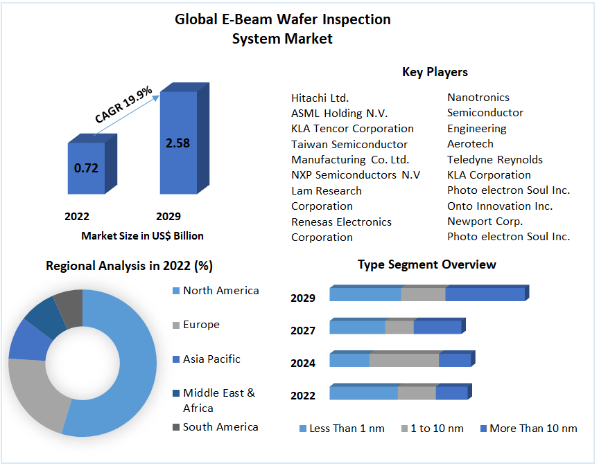
To know about the Research Methodology :- Request Free Sample Report The report study has analyzed revenue impact of COVID -19 pandemic on the sales revenue of market leaders, market followers and market disrupters in the report and same is reflected in our analysis. Increased growth of consumer electronics, smartphones and other appliances is the major factors, which are driving the overall semiconductor and electronics industry. These devices use the inspection system for detection of errors or faults in compact devices. Furthermore, the growing investments for innovations by manufactures to offer high-precision semiconductor tools with reduced cost will accelerate the industry demand. Semiconductor and electronics is one of the most dynamic industry verticals observing frequent technological advancements and miniaturization. High costs associated with the technology is impacting the growth of the e-beam wafer inspection system market. The technology consumes more time to eliminate defects compared to conventional systems due to various projection and analysis process. Moreover, these systems require highly skilled technicians to operate the equipment, resulting in increasing labor and production costs are restraining the overall market growth Manufacturers in the E-beam wafer inspection system are focusing on competitive pricing as the strategy to capture significant market share. Moreover, strategic mergers and acquisitions and technological innovations are also the key focus areas of the manufacturers.

E-Beam Wafer Inspection System Market Segmentation Analysis:

Based on the product types, the E-beam wafer inspection system market is segmented into less than 1 nm, 1 nm to 10 nm and more than 10 nm. The more than 10nm segment is expected to grow at the largest CAGR of xx% during the forecast period. These systems help in identifying small errors in compact devices and minimizes the charging of wafer surface by providing clear and sharp image of defects, which has led to its increased adoption in number of miniaturized wafers. These systems can operate in range of above 10nm to address the defect issues making them highly suitable for inspecting smaller electronics devices.

E-Beam Wafer Inspection System Market Regional Analysis:

Geographically, Asia pacific held the largest market share of 60% in overall market in 2018 owing to presence of large number semiconductor manufacturing industries. There has been an increasing adoption of these systems by semiconductor manufacturers for high-quality inspection. Rise in semiconductor industry and extending production capacity is resulting in high demand for effective wafer inspection systems. Moreover, the increasing financial support from government to invest in the construction of large number of semiconductor fabrication plants in the region, will drive the industry. A report covers the recent development in market for E-beam wafer inspection system like in February 2022, KLA Corporation developed in-line automatic defect classification (iADC) technology for its e beam wafer inspection system. The technology enables the ability to detect electrical failures within the device in the manufacturing process. The objective of the report is to present comprehensive analysis of global E-beam wafer inspection system market including all the stakeholders of the industry. The past and current status of the industry with forecasted market size and trends are presented in the report with the analysis of complicated data in simple language. The report covers the all the aspects of industry with dedicated study of key players that includes market leaders, followers and new entrants by region. PORTER, SVOR, PESTEL analysis with the potential impact of micro-economic factors by region on the market have been presented in the report. External as well as internal factors that are supposed to affect the business positively or negatively have been analyzed, which will give clear futuristic view of the industry to the decision makers. The report also helps in understanding global E-beam wafer inspection system market dynamics, structure by analyzing the market segments, and project the global E-beam wafer inspection system market size. Clear representation of competitive analysis of key players by inspection system type, price, financial position, product portfolio, growth strategies, and regional presence in the global E-beam wafer inspection system market make the report investor’s guide.

Scope of the Global E-Beam Wafer Inspection System Market: Inquire before buying

Global E-Beam Wafer Inspection System Market
Report Coverage Details
Base Year: 2022 Forecast Period: 2023-2029
Historical Data: 2017 to 2022 Market Size in 2022: US $ 0.72 Bn.
Forecast Period 2023 to 2029 CAGR: 19.9% Market Size in 2029: US $ 2.58 Bn.
Segments Covered: by Type • Less Than 1 nm • 1 to 10 nm • More Than 10 nm
by Application • Defect Imaging • Lithographic Qualification • Bare Wafer OQC/IQC • Wafer Dispositioning • Reticle Quality Inspection • Inspector Recipe Optimization

E-Beam Wafer Inspection System Market, by Region

North America (United States, Canada and Mexico) • Europe (UK, France, Germany, Italy, Spain, Sweden, Austria and Rest of Europe) • Asia Pacific (China, South Korea, Japan, India, Australia, Indonesia, Malaysia, Vietnam, Taiwan, Bangladesh, Pakistan and Rest of APAC) • Middle East and Africa (South Africa, GCC, Egypt, Nigeria and Rest of ME&A) • South America (Brazil, Argentina Rest of South America)

E-Beam Wafer Inspection System Market, Key Players are:

Hitachi Ltd. • ASML Holding N.V. • KLA Tencor Corporation • Taiwan Semiconductor Manufacturing Co. Ltd. • NXP Semiconductors N.V • Lam Research Corporation • Renesas Electronics Corporation • Integrated Device Technology Inc. • Applied Materials Inc. • Synopsys Inc. • Hermes Microvision Inc. • Nanotronics • Semiconductor Engineering • Aerotech • Teledyne Reynolds • KLA Corporation • Photo electron Soul Inc. • Onto Innovation Inc. • Newport Corp. • Photo electron Soul Inc. Frequently Asked Questions: 1. Which region has the largest share in Global E-Beam Wafer Inspection System Market ? Ans: Asia Pacific region held the highest share in 2022. 2. What is the growth rate of Global E-Beam Wafer Inspection System Market ? Ans: The Global E-Beam Wafer Inspection System Market is growing at a CAGR of 19.9% during forecasting period 2023-2029. 3. What is scope of the Global E-Beam Wafer Inspection System Market report? Ans: Global E-Beam Wafer Inspection System Market report helps with the PESTEL, PORTER, COVID-19 Impact analysis, Recommendations for Investors & Leaders, and market estimation of the forecast period. 4. Who are the key players in Global E-Beam Wafer Inspection System Market ? Ans: The important key players in the Global E-Beam Wafer Inspection System Market are – Hitachi Ltd., ASML Holding N.V., KLA Tencor Corporation, Taiwan Semiconductor Manufacturing Co. Ltd., NXP Semiconductors N.V, Lam Research Corporation, Renesas Electronics Corporation, Integrated Device Technology Inc., Applied Materials Inc., Synopsys Inc., Hermes Microvision Inc., Nanotronics, Semiconductor Engineering, Aerotech, Teledyne Reynolds, KLA Corporation, Photo electron Soul Inc., Onto Innovation Inc., Newport Corp., Photo electron Soul Inc. 5. What is the study period of this Market? Ans: The Global E-Beam Wafer Inspection System Market is studied from 2022 to 2029.
Global E-Beam Wafer Inspection System Market 1. Preface 1.1. Report Scope and Market Segmentation 1.2. Research Highlights 1.3. Research Objectives 2. Assumptions and Research Methodology 2.1. Report Assumptions 2.2. Abbreviations 2.3. Research Methodology 2.3.1. Secondary Research 2.3.1.1. Secondary data 2.3.1.2. Secondary Sources 2.3.2. Primary Research 2.3.2.1. Data from Primary Sources 2.3.2.2. Breakdown of Primary Sources 3. Executive Summary: Global E-Beam Wafer Inspection System Market Size, by Market Value (US$ Bn) 4. Market Overview 4.1. Introduction 4.2. Market Indicator 4.2.1. Drivers 4.2.2. Restraints 4.2.3. Opportunities 4.2.4. Challenges 4.3. Porter’s Analysis 4.4. Value Chain Analysis 4.5. Market Risk Analysis 4.6. SWOT Analysis 4.7. Industry Trends and Emerging Technologies 4.8. Patent Registration 5. Supply Side and Demand Side Indicators 6. Global E-Beam Wafer Inspection System Market Analysis and Forecast 6.1. Global E-Beam Wafer Inspection System Market Size & Y-o-Y Growth Analysis 6.1.1. North America 6.1.2. Europe 6.1.3. Asia Pacific 6.1.4. Middle East & Africa 6.1.5. South America 7. Global E-Beam Wafer Inspection System Market Analysis and Forecast, by Type 7.1. Introduction and Definition 7.2. Key Findings 7.3. Global E-Beam Wafer Inspection System Market Value Share Analysis, by Type 7.4. Global E-Beam Wafer Inspection System Market Size (US$ Bn) Forecast, by Type 7.5. Global E-Beam Wafer Inspection System Market Analysis, by Type 7.6. Global E-Beam Wafer Inspection System Market Attractiveness Analysis, by Type 8. Global E-Beam Wafer Inspection System Market Analysis and Forecast, by Application 8.1. Introduction and Definition 8.2. Key Findings 8.3. Global E-Beam Wafer Inspection System Market Value Share Analysis, by Application 8.4. Global E-Beam Wafer Inspection System Market Size (US$ Bn) Forecast, by Application 8.5. Global E-Beam Wafer Inspection System Market Analysis, by Application 8.6. Global E-Beam Wafer Inspection System Market Attractiveness Analysis, by Application 9. Global E-Beam Wafer Inspection System Market Analysis, by Region 9.1. Global E-Beam Wafer Inspection System Market Value Share Analysis, by Region 9.2. Global E-Beam Wafer Inspection System Market Size (US$ Bn) Forecast, by Region 9.3. Global E-Beam Wafer Inspection System Market Attractiveness Analysis, by Region 10. North America E-Beam Wafer Inspection System Market Analysis 10.1. Key Findings 10.2. North America E-Beam Wafer Inspection System Market Overview 10.3. North America E-Beam Wafer Inspection System Market Value Share Analysis, by Type 10.4. North America E-Beam Wafer Inspection System Market Forecast, by Type 10.4.1. Less Than 1 nm 10.4.2. 1 to 10 nm 10.4.3. More Than 10 nm 10.5. North America E-Beam Wafer Inspection System Market Value Share Analysis, by Application 10.6. North America E-Beam Wafer Inspection System Market Forecast, by Application 10.6.1. Defect Imaging 10.6.2. Lithographic Qualification 10.6.3. Bare Wafer OQC/IQC 10.6.4. Wafer Dispositioning 10.6.5. Reticle Quality Inspection 10.6.6. Inspector Recipe Optimization 10.7. North America E-Beam Wafer Inspection System Market Value Share Analysis, by Country 10.8. North America E-Beam Wafer Inspection System Market Forecast, by Country 10.8.1. U.S. 10.8.2. Canada 10.9. North America E-Beam Wafer Inspection System Market Analysis, by Country 10.10. U.S. E-Beam Wafer Inspection System Market Forecast, by Type 10.10.1. Less Than 1 nm 10.10.2. 1 to 10 nm 10.10.3. More Than 10 nm 10.11. U.S. E-Beam Wafer Inspection System Market Forecast, by Application 10.11.1. Defect Imaging 10.11.2. Lithographic Qualification 10.11.3. Bare Wafer OQC/IQC 10.11.4. Wafer Dispositioning 10.11.5. Reticle Quality Inspection 10.11.6. Inspector Recipe Optimization 10.12. Canada E-Beam Wafer Inspection System Market Forecast, by Type 10.12.1. Less Than 1 nm 10.12.2. 1 to 10 nm 10.12.3. More Than 10 nm 10.13. Canada E-Beam Wafer Inspection System Market Forecast, by Application 10.13.1. Defect Imaging 10.13.2. Lithographic Qualification 10.13.3. Bare Wafer OQC/IQC 10.13.4. Wafer Dispositioning 10.13.5. Reticle Quality Inspection 10.13.6. Inspector Recipe Optimization 10.14. North America E-Beam Wafer Inspection System Market Attractiveness Analysis 10.14.1. By Type 10.14.2. By Application 10.15. PEST Analysis 10.16. Key Trends 10.17. Key Development 11. Europe E-Beam Wafer Inspection System Market Analysis 11.1. Key Findings 11.2. Europe E-Beam Wafer Inspection System Market Overview 11.3. Europe E-Beam Wafer Inspection System Market Value Share Analysis, by Type 11.4. Europe E-Beam Wafer Inspection System Market Forecast, by Type 11.4.1. Less Than 1 nm 11.4.2. 1 to 10 nm 11.4.3. More Than 10 nm 11.5. Europe E-Beam Wafer Inspection System Market Value Share Analysis, by Application 11.6. Europe E-Beam Wafer Inspection System Market Forecast, by Application 11.6.1. Defect Imaging 11.6.2. Lithographic Qualification 11.6.3. Bare Wafer OQC/IQC 11.6.4. Wafer Dispositioning 11.6.5. Reticle Quality Inspection 11.6.6. Inspector Recipe Optimization 11.7. Europe E-Beam Wafer Inspection System Market Value Share Analysis, by Country 11.8. Europe E-Beam Wafer Inspection System Market Forecast, by Country 11.8.1. Germany 11.8.2. U.K. 11.8.3. France 11.8.4. Italy 11.8.5. Spain 11.8.6. Rest of Europe 11.9. Europe E-Beam Wafer Inspection System Market Analysis, by Country 11.10. Germany E-Beam Wafer Inspection System Market Forecast, by Type 11.10.1. Less Than 1 nm 11.10.2. 1 to 10 nm 11.10.3. More Than 10 nm 11.11. Germany E-Beam Wafer Inspection System Market Forecast, by Application 11.11.1. Defect Imaging 11.11.2. Lithographic Qualification 11.11.3. Bare Wafer OQC/IQC 11.11.4. Wafer Dispositioning 11.11.5. Reticle Quality Inspection 11.11.6. Inspector Recipe Optimization 11.12. U.K. E-Beam Wafer Inspection System Market Forecast, by Type 11.12.1. Less Than 1 nm 11.12.2. 1 to 10 nm 11.12.3. More Than 10 nm 11.13. U.K. E-Beam Wafer Inspection System Market Forecast, by Application 11.13.1. Defect Imaging 11.13.2. Lithographic Qualification 11.13.3. Bare Wafer OQC/IQC 11.13.4. Wafer Dispositioning 11.13.5. Reticle Quality Inspection 11.13.6. Inspector Recipe Optimization 11.14. France E-Beam Wafer Inspection System Market Forecast, by Type 11.14.1. Less Than 1 nm 11.14.2. 1 to 10 nm 11.14.3. More Than 10 nm 11.15. France E-Beam Wafer Inspection System Market Forecast, by Application 11.15.1. Defect Imaging 11.15.2. Lithographic Qualification 11.15.3. Bare Wafer OQC/IQC 11.15.4. Wafer Dispositioning 11.15.5. Reticle Quality Inspection 11.15.6. Inspector Recipe Optimization 11.16. Italy E-Beam Wafer Inspection System Market Forecast, by Type 11.16.1. Less Than 1 nm 11.16.2. 1 to 10 nm 11.16.3. More Than 10 nm 11.17. Italy E-Beam Wafer Inspection System Market Forecast, by Application 11.17.1. Defect Imaging 11.17.2. Lithographic Qualification 11.17.3. Bare Wafer OQC/IQC 11.17.4. Wafer Dispositioning 11.17.5. Reticle Quality Inspection 11.17.6. Inspector Recipe Optimization 11.18. Spain E-Beam Wafer Inspection System Market Forecast, by Type 11.18.1. Less Than 1 nm 11.18.2. 1 to 10 nm 11.18.3. More Than 10 nm 11.19. Spain E-Beam Wafer Inspection System Market Forecast, by Application 11.19.1. Defect Imaging 11.19.2. Lithographic Qualification 11.19.3. Bare Wafer OQC/IQC 11.19.4. Wafer Dispositioning 11.19.5. Reticle Quality Inspection 11.19.6. Inspector Recipe Optimization 11.20. Rest of Europe E-Beam Wafer Inspection System Market Forecast, by Type 11.20.1. Less Than 1 nm 11.20.2. 1 to 10 nm 11.20.3. More Than 10 nm 11.21. Rest of Europe E-Beam Wafer Inspection System Market Forecast, by Application 11.21.1. Defect Imaging 11.21.2. Lithographic Qualification 11.21.3. Bare Wafer OQC/IQC 11.21.4. Wafer Dispositioning 11.21.5. Reticle Quality Inspection 11.21.6. Inspector Recipe Optimization 11.22. Europe E-Beam Wafer Inspection System Market Attractiveness Analysis 11.22.1. By Type 11.22.2. By Application 11.23. PEST Analysis 11.24. Key Trend 11.25. Key Development 12. Asia Pacific E-Beam Wafer Inspection System Market Analysis 12.1. Key Findings 12.2. Asia Pacific E-Beam Wafer Inspection System Market Overview 12.3. Asia Pacific E-Beam Wafer Inspection System Market Value Share Analysis, by Type 12.4. Asia Pacific E-Beam Wafer Inspection System Market Forecast, by Type 12.4.1. Less Than 1 nm 12.4.2. 1 to 10 nm 12.4.3. More Than 10 nm 12.5. Asia Pacific E-Beam Wafer Inspection System Market Value Share Analysis, by Application 12.6. Asia Pacific E-Beam Wafer Inspection System Market Forecast, by Application 12.6.1. Defect Imaging 12.6.2. Lithographic Qualification 12.6.3. Bare Wafer OQC/IQC 12.6.4. Wafer Dispositioning 12.6.5. Reticle Quality Inspection 12.6.6. Inspector Recipe Optimization 12.7. Asia Pacific E-Beam Wafer Inspection System Market Value Share Analysis, by Country 12.8. Asia Pacific E-Beam Wafer Inspection System Market Forecast, by Country 12.8.1. China 12.8.2. India 12.8.3. Japan 12.8.4. ASEAN 12.8.5. Rest of Asia Pacific 12.9. Asia Pacific E-Beam Wafer Inspection System Market Analysis, by Country 12.10. China E-Beam Wafer Inspection System Market Forecast, by Type 12.10.1. Less Than 1 nm 12.10.2. 1 to 10 nm 12.10.3. More Than 10 nm 12.11. China E-Beam Wafer Inspection System Market Forecast, by Application 12.11.1. Defect Imaging 12.11.2. Lithographic Qualification 12.11.3. Bare Wafer OQC/IQC 12.11.4. Wafer Dispositioning 12.11.5. Reticle Quality Inspection 12.11.6. Inspector Recipe Optimization 12.12. India E-Beam Wafer Inspection System Market Forecast, by Type 12.12.1. Less Than 1 nm 12.12.2. 1 to 10 nm 12.12.3. More Than 10 nm 12.13. India E-Beam Wafer Inspection System Market Forecast, by Application 12.13.1. Defect Imaging 12.13.2. Lithographic Qualification 12.13.3. Bare Wafer OQC/IQC 12.13.4. Wafer Dispositioning 12.13.5. Reticle Quality Inspection 12.13.6. Inspector Recipe Optimization 12.14. Japan E-Beam Wafer Inspection System Market Forecast, by Type 12.14.1. Less Than 1 nm 12.14.2. 1 to 10 nm 12.14.3. More Than 10 nm 12.15. Japan E-Beam Wafer Inspection System Market Forecast, by Application 12.15.1. Defect Imaging 12.15.2. Lithographic Qualification 12.15.3. Bare Wafer OQC/IQC 12.15.4. Wafer Dispositioning 12.15.5. Reticle Quality Inspection 12.15.6. Inspector Recipe Optimization 12.16. ASEAN E-Beam Wafer Inspection System Market Forecast, by Type 12.16.1. Less Than 1 nm 12.16.2. 1 to 10 nm 12.16.3. More Than 10 nm 12.17. ASEAN E-Beam Wafer Inspection System Market Forecast, by Application 12.17.1. Defect Imaging 12.17.2. Lithographic Qualification 12.17.3. Bare Wafer OQC/IQC 12.17.4. Wafer Dispositioning 12.17.5. Reticle Quality Inspection 12.17.6. Inspector Recipe Optimization 12.18. Rest of Asia Pacific E-Beam Wafer Inspection System Market Forecast, by Type 12.18.1. Less Than 1 nm 12.18.2. 1 to 10 nm 12.18.3. More Than 10 nm 12.18.4. Pharmaceuticals 12.19. Rest of Asia Pacific E-Beam Wafer Inspection System Market Forecast, by Application 12.19.1. Defect Imaging 12.19.2. Lithographic Qualification 12.19.3. Bare Wafer OQC/IQC 12.19.4. Wafer Dispositioning 12.19.5. Reticle Quality Inspection 12.19.6. Inspector Recipe Optimization 12.20. Asia Pacific E-Beam Wafer Inspection System Market Attractiveness Analysis 12.20.1. By Type 12.20.2. By Application 12.21. PEST Analysis 12.22. Key Trend 12.23. Key Development 13. Middle East & Africa E-Beam Wafer Inspection System Market Analysis 13.1. Key Findings 13.2. Middle East & Africa E-Beam Wafer Inspection System Market Overview 13.3. Middle East & Africa E-Beam Wafer Inspection System Market Value Share Analysis, by Type 13.4. Middle East & Africa E-Beam Wafer Inspection System Market Forecast, by Type 13.4.1. Less Than 1 nm 13.4.2. 1 to 10 nm 13.4.3. More Than 10 nm 13.5. Middle East & Africa E-Beam Wafer Inspection System Market Value Share Analysis, by Application 13.6. Middle East & Africa E-Beam Wafer Inspection System Market Forecast, by Application 13.6.1. Defect Imaging 13.6.2. Lithographic Qualification 13.6.3. Bare Wafer OQC/IQC 13.6.4. Wafer Dispositioning 13.6.5. Reticle Quality Inspection 13.6.6. Inspector Recipe Optimization 13.7. Middle East & Africa E-Beam Wafer Inspection System Market Value Share Analysis, by Country 13.8. Middle East & Africa E-Beam Wafer Inspection System Market Forecast, by Country 13.8.1. GCC 13.8.2. South Africa 13.8.3. Rest of Middle East & Africa 13.9. Middle East & Africa E-Beam Wafer Inspection System Market Analysis, by Country 13.10. GCC E-Beam Wafer Inspection System Market Forecast, by Type 13.10.1. Less Than 1 nm 13.10.2. 1 to 10 nm 13.10.3. More Than 10 nm 13.11. GCC E-Beam Wafer Inspection System Market Forecast, by Application 13.11.1. Defect Imaging 13.11.2. Lithographic Qualification 13.11.3. Bare Wafer OQC/IQC 13.11.4. Wafer Dispositioning 13.11.5. Reticle Quality Inspection 13.11.6. Inspector Recipe Optimization 13.12. South Africa E-Beam Wafer Inspection System Market Forecast, by Type 13.12.1. Less Than 1 nm 13.12.2. 1 to 10 nm 13.12.3. More Than 10 nm 13.13. South Africa E-Beam Wafer Inspection System Market Forecast, by Application 13.13.1. Defect Imaging 13.13.2. Lithographic Qualification 13.13.3. Bare Wafer OQC/IQC 13.13.4. Wafer Dispositioning 13.13.5. Reticle Quality Inspection 13.13.6. Inspector Recipe Optimization 13.14. Rest of Middle East & Africa E-Beam Wafer Inspection System Market Forecast, by Type 13.14.1. Less Than 1 nm 13.14.2. 1 to 10 nm 13.14.3. More Than 10 nm 13.15. Rest of Middle East & Africa E-Beam Wafer Inspection System Market Forecast, by Application 13.15.1. Defect Imaging 13.15.2. Lithographic Qualification 13.15.3. Bare Wafer OQC/IQC 13.15.4. Wafer Dispositioning 13.15.5. Reticle Quality Inspection 13.15.6. Inspector Recipe Optimization 13.16. Middle East & Africa E-Beam Wafer Inspection System Market Attractiveness Analysis 13.16.1. By Type 13.16.2. By Application 13.17. PEST Analysis 13.18. Key Trend 13.19. Key Development 14. South America E-Beam Wafer Inspection System Market Analysis 14.1. Key Findings 14.2. South America E-Beam Wafer Inspection System Market Overview 14.3. South America E-Beam Wafer Inspection System Market Value Share Analysis, by Type 14.4. South America E-Beam Wafer Inspection System Market Forecast, by Type 14.4.1. Less Than 1 nm 14.4.2. 1 to 10 nm 14.4.3. More Than 10 nm 14.5. Others South America E-Beam Wafer Inspection System Market Value Share Analysis, by Application 14.6. South America E-Beam Wafer Inspection System Market Forecast, by Application 14.6.1. Defect Imaging 14.6.2. Lithographic Qualification 14.6.3. Bare Wafer OQC/IQC 14.6.4. Wafer Dispositioning 14.6.5. Reticle Quality Inspection 14.6.6. Inspector Recipe Optimization 14.7. South America E-Beam Wafer Inspection System Market Value Share Analysis, by Country 14.8. South America E-Beam Wafer Inspection System Market Forecast, by Country 14.8.1. Brazil 14.8.2. Mexico 14.8.3. Rest of South America 14.9. Brazil E-Beam Wafer Inspection System Market Forecast, by Type 14.9.1. Less Than 1 nm 14.9.2. 1 to 10 nm 14.9.3. More Than 10 nm 14.10. Brazil E-Beam Wafer Inspection System Market Forecast, by Application 14.10.1. Defect Imaging 14.10.2. Lithographic Qualification 14.10.3. Bare Wafer OQC/IQC 14.10.4. Wafer Dispositioning 14.10.5. Reticle Quality Inspection 14.10.6. Inspector Recipe Optimization 14.11. Mexico E-Beam Wafer Inspection System Market Forecast, by Type 14.11.1. Less Than 1 nm 14.11.2. 1 to 10 nm 14.11.3. More Than 10 nm 14.12. Mexico E-Beam Wafer Inspection System Market Forecast, by Application 14.12.1. Defect Imaging 14.12.2. Lithographic Qualification 14.12.3. Bare Wafer OQC/IQC 14.12.4. Wafer Dispositioning 14.12.5. Reticle Quality Inspection 14.12.6. Inspector Recipe Optimization 14.13. Rest of South America E-Beam Wafer Inspection System Market Forecast, by Type 14.13.1. Less Than 1 nm 14.13.2. 1 to 10 nm 14.13.3. More Than 10 nm 14.14. Rest of South America E-Beam Wafer Inspection System Market Forecast, by Application 14.14.1. Defect Imaging 14.14.2. Lithographic Qualification 14.14.3. Bare Wafer OQC/IQC 14.14.4. Wafer Dispositioning 14.14.5. Reticle Quality Inspection 14.14.6. Inspector Recipe Optimization 14.15. South America E-Beam Wafer Inspection System Market Attractiveness Analysis 14.15.1. By Type 14.15.2. By Application 14.16. PEST Analysis 14.17. Key Trend 14.18. Key Development 15. Company Profiles 15.1. Market Share Analysis, by Company 15.2. Competition Matrix 15.2.1. Competitive Benchmarking of key players by price, presence, market share, Applications and R&D investment 15.2.2. New Product Launches and Product Enhancements 15.2.3. Market Consolidation 15.2.3.1. M&A by Regions, Investment and Applications 15.2.3.2. M&A Key Players, Forward Integration and Backward Integration 15.3. Company Profiles: Key Players 15.3.1. Hitachi Ltd. 15.3.1.1. Company Overview 15.3.1.2. Financial Overview 15.3.1.3. Product Portfolio 15.3.1.4. Business Strategy 15.3.1.5. Recent Developments 15.3.1.6. Company Footprint 15.3.2. ASML Holding N.V. 15.3.3. KLA Tencor Corporation 15.3.4. Taiwan Semiconductor Manufacturing Co. Ltd. 15.3.5. NXP Semiconductors N.V 15.3.6. Lam Research Corporation 15.3.7. Renesas Electronics Corporation 15.3.8. Integrated Device Technology Inc. 15.3.9. Applied Materials Inc. 15.3.10. Synopsys Inc. 15.3.11. Hermes Microvision Inc. 15.3.12. Nanotronics 15.3.13. Semiconductor Engineering 15.3.14. Aerotech 15.3.15. Teledyne Reynolds 15.3.16. KLA Corporation 15.3.17. Photo electron Soul Inc. 15.3.18. Onto Innovation Inc. 15.3.19. Newport Corp. 15.3.20. Photo electron Soul Inc. 16. Primary Key Insights
  • INQUIRE BEFORE BUYING