
KLA Corporation Controls Over 56% of the Market That Makes AI Chips Possible and It Is Still Pulling Away from the Field
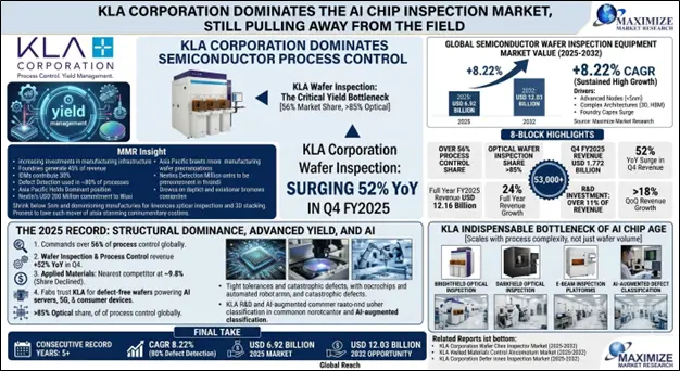
The global Semiconductor Wafer Inspection Equipment Market was valued at USD 6.92 Billion in 2025 and is projected to reach USD 12.03 Billion by 2032, growing at a CAGR of 8.22%, per Maximize Market Research. KLA Corporation, the undisputed market leader commanding over 56% of the global process control segment, reported wafer inspection revenue surging 52% year-over-year in Q4 FY2025, as AI-driven chip complexity makes precision defect detection not just essential, but non-negotiable.
There is a piece of equipment that stands between a USD 50,000 silicon wafer and a defective chip that no one can use. That equipment is a wafer inspection system. And the company that dominates this market is KLA Corporation.
The Global Semiconductor Wafer Inspection Equipment Market was valued at USD 6.92 Billion in 2025 and is expected to reach USD 12.03 Billion by 2032, expanding at a CAGR of 8.22% during the forecast period, according to Maximize Market Research. KLA is the company that a majority of the world’s most advanced semiconductor fabs trust to make sure their wafers are defect-free before they become chips that power AI servers, 5G networks, and consumer devices.
The Numbers That Define a Monopoly in Motion
KLA’s dominance in semiconductor wafer inspection is not incremental — it is structural. The company commands over 56% of the overall semiconductor process control, metrology, and inspection segment globally. In optical wafer inspection, its market share exceeds 85%. In the fourth quarter of fiscal year 2025, KLA’s wafer inspection and process control revenue reached USD 1.772 billion, a 52% surge year-over-year and an 18% jump quarter-over-quarter. Full fiscal year 2025 revenue was approximately USD 12.16 billion, representing approximately 24% year-on-year growth, driven by AI infrastructure buildout at leading foundries.
Its nearest competitor, Applied Materials, holds approximately 9.8% of the global metrology and inspection market, a share that actually declined in 2025, even as KLA’s expanded. Every major competitor lost share to KLA in 2025, according to independent market analysis. This is not a close race.
Why Wafer Inspection Is the Indispensable Bottleneck of the AI Chip Age
As semiconductor nodes shrink below 5 nanometers and chip architectures incorporate 3D stacking, chiplets, and high-bandwidth memory, the number of process steps that require inspection multiplies. Unlike conventional equipment that scales with wafer volume, inspection and metrology tools scale with process complexity. The more steps, the tighter the tolerances, the more catastrophic an undetected defect — and therefore the more inspection equipment a leading fab must deploy. This dynamic is structurally favorable for KLA at every advanced node transition.
KLA invests over 11% of its annual revenue in research and development. Its AI-augmented defect classification systems, brightfield and darkfield optical inspection platforms, and e-beam inspection tools are now integral to the yield management strategies of TSMC, Samsung, and Intel, which together represent a significant concentration of the company’s revenue base.
MMR Insight: The Semiconductor Wafer Inspection Equipment Market is driven by increasing investments in semiconductor manufacturing infrastructure globally. Foundries generate approximately 45% of market revenue, while Integrated Device Manufacturers contribute approximately 30%. Defect detection is used in approximately 80% of all wafer inspection processes. Asia Pacific holds the dominant regional position, with the region accounting for the largest share of global semiconductor manufacturing capacity, anchored by Taiwan, South Korea, Japan, and China. Strategic investments such as Nextin’s USD 200 million commitment to establish inspection equipment operations in Wuxi, China reflect the intensity of regional competition now emerging in the inspection equipment segment.
Final Take
The Semiconductor Wafer Inspection Equipment Market growing from USD 6.92 Billion in 2025 to USD 12.03 Billion by 2032 at an 8.22% CAGR is, at its core, a story about the physics of advanced chip manufacturing. The smaller the node, the more inspection it requires. The more complex the package, the more yield management it demands. KLA Corporation has built its business model around precisely this logic. Its technology, its market share, and its financial performance all point in the same direction: as the AI era makes semiconductor manufacturing more complex, KLA becomes more indispensable. That is a competitive position that is extremely difficult to dislodge.
Related Reports
Explore related market intelligence reports from Maximize Market Research: