
Chiplets Market Size by Die Type, Integration Technology, End Use and Packaging Platform
Overview
Chiplets Market Key Highlights
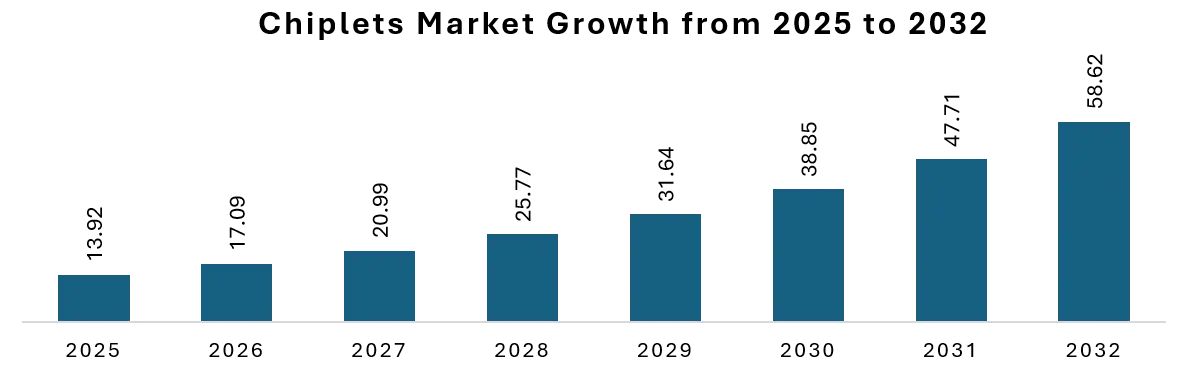
1. The Global Chiplets Market is estimated to surge from USD 13.92 Bn 2025 to USD 58.62 Bn by 2032, expanding at an exceptional CAGR of 22.8% driven by the exponential rise of artificial intelligence workloads, heterogeneous integration breakthroughs, and the semiconductor industry's structural shift away from monolithic die architectures toward modular, yield-optimized chiplet ecosystems.
2. North America commands the largest market share, while Asia Pacific registers the fastest growth, with Taiwan, South Korea, China, and Japan emerging as critical chiplet manufacturing and packaging hubs, propelled by massive foundry investment cycles and government-backed semiconductor sovereignty programs.
3. AI accelerator chiplets and high-bandwidth memory (HBM) die stacking dominate the high-value premium segment, while logic chiplets, analog mixed-signal dies, and photonic interconnect chiplets are rapidly diversifying the addressable design space across hyperscaler, automotive, and telecom applications.
4. Advanced packaging platforms including TSMC's CoWoS and SoIC, Intel's EMIB and Foveros, Samsung's X-Cube, and ASE Group's VIPack are emerging as the critical infrastructure layer enabling chiplet-to-chiplet integration at semiconductor-grade bandwidth and power efficiency.
5. The UCIe (Universal Chiplet Interconnect Express) consortium's open-standard momentum, die-to-die PHY standardization, and growing adoption of 2.5D and 3D packaging are accelerating cross-vendor chiplet ecosystem development, reshaping IP licensing models and supply chain architecture across the global semiconductor industry.
Chiplets Market Overview
The global Chiplets Market stands at the epicenter of the most profound transformation in semiconductor design since the advent of the integrated circuit itself. What began as an engineering workaround for yield limitations in large monolithic dies has evolved into a foundational architectural paradigm, reshaping how the world's most sophisticated chips are designed, manufactured, and assembled.
In 2025, the chiplets market was valued at USD 13.92 Bn 2025 to USD 58.62 Bn by 2032, expanding at an exceptional CAGR of 22.8%. This extraordinary growth trajectory reflects a fundamental rethinking of Moore's Law economics: as monolithic scaling becomes physically and economically prohibitive beyond advanced nodes, chiplets offer a path to continued performance scaling through architectural innovation rather than pure transistor density. The convergence of AI compute demand, advanced packaging capabilities, and open-standard interconnect protocols has transformed chiplets from a niche engineering strategy into the defining semiconductor megatrend of the decade.
To know about the Research Methodology :- Request Free Sample Report
Chiplets Market, Key Drivers
Chiplets Market Growth is primarily catalyzed by the insatiable compute demands of artificial intelligence training and inference workloads, where the physical limits of monolithic die area collide with exponentially growing transistor requirements. Leading AI accelerator architects at NVIDIA, AMD, Google, and emerging custom silicon teams at Microsoft, Amazon, Meta, and Apple are increasingly designing products as multi-die assemblies, with chiplets enabling the disaggregation of compute, memory, I/O, and analog functions across specialized process nodes.
The demonstrated performance, power, and cost advantages of heterogeneous integration in flagship products such as AMD's EPYC processors and MI300 AI accelerators have unambiguously validated the chiplet architectural paradigm for mainstream high-volume semiconductor design. Additionally, the mounting difficulty and capital expenditure of leading-edge node manufacturing at 3nm and beyond are making chiplet-based yield optimization an economic imperative rather than a design choice, further accelerating the industrial adoption across hyperscaler, enterprise, and edge compute market segments.
Chiplets Market Restraints
Despite the compelling growth narrative, the Chiplets Market faces significant challenges rooted in the technical complexity of die-to-die integration. Achieving semiconductor-grade signal integrity, power delivery uniformity, and thermal management across heterogeneous chiplet assemblies requires advanced packaging infrastructure whose capital cost and engineering sophistication remain accessible only to a small number of well-capitalized semiconductor companies and OSATs.
The absence of universally adopted chiplet interconnect standards, while addressed in principle by the UCIe consortium, continues to limit cross-vendor chiplet sourcing and IP reuse, constraining the development of an open chiplet marketplace analogous to mature PCB component ecosystems. Testing complexity across chiplet boundaries, known-good-die (KGD) qualification requirements, and the challenge of chiplet-aware EDA toolchains represent substantial barriers to adoption for fabless semiconductor companies without dedicated advanced packaging engineering teams, limiting the speed at which Chiplets Market Growth can penetrate mid-market and consumer electronics design cycles.
Chiplets Market Opportunities
Chiplets Market are expanding across a remarkably diverse horizon of application and technology vectors. The emergence of photonic chiplets integrating silicon photonic interconnect dies with electronic processing chiplets promises to unlock bandwidth-density improvements of 10 to 100 times over conventional copper interconnects, positioning photonic integration as the next frontier of chiplet innovation for data center and HPC applications.
Automotive-grade chiplet platforms, designed to meet AEC-Q100 reliability standards while enabling software-defined vehicle architectures through modular compute disaggregation, represent a rapidly maturing opportunity as Tier 1 suppliers and OEMs accelerate centralized vehicle compute platform deployments. Furthermore, the emergence of open chiplet foundry services, reusable analog and SerDes chiplet IP libraries, and DARPA-funded heterogeneous integration research programs is creating a nascent chiplet ecosystem infrastructure that promises to dramatically lower entry barriers and accelerate the forecast toward sustained long-term growth, particularly in defense, aerospace, and industrial IoT verticals demanding high-reliability disaggregated semiconductor solutions.
Emerging Trends Shaping the Chiplets Industry
Chiplets Market Trends reveal an industry in the midst of a fundamental architectural reimagination, where the silicon system of record is no longer a single die but a carefully curated assembly of best-in-class functional tiles. The emergence of standardized chiplet interconnect fabrics under the UCIe 1.0 and evolving UCIe 2.0 specifications is creating the technical foundation for a chiplet marketplace where dies from TSMC, Intel, Samsung, and GlobalFoundries can be composed into system solutions by fabless companies without requiring custom die-to-die interface co-design. Simultaneously, 3D stacking technologies including hybrid bonding at sub-micron pitch are enabling face-to-face die stacking with connectivity densities exceeding one million connections per square millimeter, unlocking memory-on-logic bandwidth that fundamentally changes the memory wall constraint for AI accelerators and high-performance CPUs.
Another defining trend is the rapid expansion of the chiplet IP licensing ecosystem, where companies like Arm, Rambus, Cadence, and Synopsys are developing chiplet-ready PHY, SerDes, and controller IP blocks pre-characterized for integration in chiplet assemblies on advanced packaging substrates. The growing investment in AI-driven chiplet design automation, including floorplanning, signal integrity simulation, and thermal modeling tools purpose-built for multi-die assemblies, is progressively lowering the engineering barrier and compressing chiplet design cycles from years to months, further transforming the Chiplets Industry Outlook and enabling a broader universe of semiconductor companies to access the architectural and economic advantages of chiplet-based system design.
Chiplets Market Manufacturing Cost & Pricing Analysis
The advanced packaging substrate and interposer segment represents the single largest incremental cost driver in the Chiplets Market value chain, characterized by the extreme precision requirements of silicon interposers, organic substrates with ultra-fine line spacing, and glass interposer platforms capable of routing thousands of die-to-die connections at micron-scale pitch. TSMC CoWoS silicon interposer packaging commands a significant cost premium over conventional flip-chip BGA assembly, with the interposer substrate alone representing 15 to 35 percent of total package cost for high-end AI accelerator and HPC chiplet assemblies, reflecting the capital intensity of lithography-defined substrate routing, under-bump metallization, micro-bump plating, and underfill processing at advanced packaging fabs.
• Silicon interposer substrates for 2.5D integration carry manufacturing costs of USD 800 to 4,500 per interposer unit depending on reticle field size, routing layer count, and micro-bump density, reflecting extreme precision lithography requirements and low-volume production economics at leading-edge packaging fabs.
• Advanced organic substrates for fan-out wafer-level packaging (FOWLP) and embedded multi-die interconnect bridge (EMIB) solutions are priced at USD 150 to 800 per substrate, representing a cost advantage over silicon interposers while sacrificing interconnect density at the die-to-die boundary.
• Known-good-die (KGD) qualification, pre-assembly wafer-level testing, and chiplet burn-in screening add 8 to 20 percent to component cost but are essential for achieving acceptable multi-chiplet assembly yield, as unscreened die-level defects compound multiplicatively across the chiplet count in a complex assembly.
• Pricing for complete chiplet-based semiconductor packages carries a 2 to 4 times premium over equivalent-function monolithic solutions, reflecting advanced packaging process cost, lower initial yield, and engineering investment amortization, partially offset by the silicon area and node cost optimization benefits achieved through chiplet disaggregation.
Chiplet Die Manufacturing & Process Node Cost Analysis
The chiplet die manufacturing cost structure reflects one of the primary economic motivations for chiplet adoption: the ability to manufacture each functional tile on the most cost-optimal process node for its specific circuit type rather than constraining the entire design to the most advanced and expensive node available. Compute chiplets targeting AI and CPU workloads are manufactured at leading-edge nodes (3nm to 5nm) commanding wafer costs of USD 17,000 to 22,000 per wafer, while I/O, analog, and SerDes chiplets can be manufactured at mature nodes (28nm to 7nm) at wafer costs of USD 3,000 to 9,000, yielding a blended system cost significantly below what an equivalent monolithic SoC at the leading edge would require. This node-optimization capability is a structurally important cost advantage that the Chiplets Market Analysis identifies as a central driver of chiplet adoption economics across hyperscaler custom silicon and merchant semiconductor segments alike.
Chiplets Market Regional Insights
North America Chiplets Market - Innovation & Hyperscaler Demand Leader
North America dominates the Chiplets Market, anchored by the unparalleled concentration of semiconductor design leadership, hyperscaler custom silicon programs, and advanced packaging R&D investment in the United States. NVIDIA's Blackwell GPU architecture, AMD's EPYC Genoa and MI300X AI accelerator platforms, Intel's Meteor Lake consumer processor and Ponte Vecchio HPC GPU, and Apple's M-series system-on-package designs collectively represent the world's highest-value chiplet integration programs, driving both technology advancement and advanced packaging demand at TSMC, Intel Foundry Services, and Amkor Technology.
The CHIPS and Science Act's USD 39 billion in semiconductor manufacturing incentives is catalyzing a wave of domestic advanced packaging capacity investment from TSMC Arizona, Intel Ohio, and Samsung Texas that will progressively reduce North America's historical dependence on Asian advanced packaging supply chains, creating a more resilient and geographically diversified Chiplets Market Revenue base across the region.
Asia Pacific Chiplets Market - Manufacturing Backbone & Fastest Growing Region
Asia Pacific commands the world's most critical chiplet manufacturing infrastructure, with Taiwan's TSMC operating the globally dominant CoWoS and SoIC advanced packaging platforms that underpin virtually every high-volume AI accelerator chiplet production program. South Korea's Samsung and SK Hynix lead in HBM memory die stacking and 3D DRAM integration, components that are structurally inseparable from the chiplet ecosystem in AI accelerator and HPC applications.
The Asia Pacific Chiplets Market is also witnessing aggressive domestic chiplet ecosystem development in China, where Huawei, Alibaba, Biren Technology, and Moore Threads are pursuing chiplet-based design strategies as a path to competitive high-end compute performance within the constraints imposed by US export control restrictions on advanced semiconductor equipment and leading-edge node access. Japan's renewed semiconductor ambition, embodied in the Rapidus 2nm program and government-backed LSTC research consortium, is positioning the country as a future chiplet technology contributor, particularly in advanced substrate and interconnect innovation, supporting the region's claim to the highest Chiplets Market Size growth trajectory through 2032.
Europe Chiplets Market - Strategic Sovereignty & Automotive Integration
Europe's Chiplets Market is shaped by the region's strategic imperative to reduce critical semiconductor import dependence, as articulated through the European Chips Act's EUR 43 billion investment framework targeting 20 percent of global semiconductor production by 2030. Infineon Technologies, STMicroelectronics, NXP Semiconductors, and Bosch Sensortec are increasingly evaluating chiplet-based platform architectures for next-generation automotive SoCs, industrial microcontrollers, and power management ICs, drawn by chiplet's promise of functional modularity and supply chain flexibility in safety-critical application domains. Imec's advanced semiconductor research programs in Belgium, in partnership with ASML's EUV lithography ecosystem, are establishing a European center of gravity for chiplet interconnect and heterogeneous integration research that could yield significant Chiplets Industry Growth contributions in specialized automotive, defense, and industrial chiplet segments over the forecast horizon.
Middle East & Africa and South America - Strategic Investment & Emerging Adoption
The Middle East's Chiplets Market is in early formation, driven primarily by sovereign wealth fund-backed semiconductor investment programs in Saudi Arabia and the UAE, where NEOM's smart city infrastructure ambitions and the UAE's AI national strategy are creating nascent demand for advanced AI accelerator chiplet deployments in data center and edge computing applications. South America's chiplet market is nascent but strategically noteworthy, with Brazil's semiconductor industry development initiatives and growing data center investment by AWS, Google, and Microsoft creating emerging demand for chiplet-based AI inference infrastructure, positioning the region for meaningful Chiplets Market Investment Opportunities as hyperscaler infrastructure buildout accelerates across Latin American markets through the forecast period.
Chiplets Market Competitive Landscape
The Global Chiplets Market Competitive Landscape is concentrated among a small group of vertically integrated semiconductor technology leaders whose advanced packaging infrastructure, foundry capabilities, and design ecosystem depth create formidable barriers to entry. TSMC commands the most strategically critical position, operating as the primary advanced packaging foundry for the chiplet programs of Apple, NVIDIA, AMD, Broadcom, and MediaTek through its CoWoS 2.5D silicon interposer and SoIC 3D face-to-face bonding platforms. Intel pursues a distinctive integrated IDM 2.0 chiplet strategy, combining its proprietary EMIB silicon bridge and Foveros 3D die stacking technologies with an open ecosystem ambition through Intel Foundry Services.
Samsung Foundry advances chiplet integration through its X-Cube 3D stacking platform and I-Cube interposer technology, while ASE Group and Amkor Technology lead the OSAT segment in chiplet assembly and advanced substrate packaging. In the chiplet IP and ecosystem layer, Arm, Cadence, and Synopsys are critical enablers, collectively shaping the long-term Chiplets Market Share through interconnect standards, EDA toolchain innovation, and chiplet-ready IP portfolio development that will define the architectural boundaries of the Chiplets Industry through 2032 and beyond.
Chiplets Market Scope: Inquire before buying
| CHIPLETS MARKET - REPORT COVERAGE | |
| Base Year | 2025 |
| Forecast Period | 2025–2032 |
| Historical Data | 2020 to 2024 |
| Market Size in 2025 | USD 18.2 Bn |
| Forecast CAGR | 20.4% |
| Market Size in 2032 | USD 78.6 Bn |
| By Die Type | Logic Chiplets |
| Memory Die (HBM, SRAM, LPDDR) | |
| Analog & Mixed-Signal Chiplets | |
| I/O & SerDes Chiplets | |
| Photonic Chiplets | |
| AI/ML Accelerator Chiplets | |
| By Integration Technology | 2.5D Silicon Interposer |
| 2.5D Embedded Bridge | |
| 3D WoW & DoW | |
| Hybrid Bonding | |
| FOWLP/InFO | |
| Co-Packaged Optics | |
| By End Use | Data Centers & HPC |
| AI Accelerators | |
| Consumer Electronics | |
| Automotive (ADAS, SDV) | |
| Telecom & 5G | |
| Defense & Aerospace | |
| Industrial & IoT | |
| By Packaging Platform | TSMC CoWoS & SoIC |
| Intel EMIB & Foveros | |
| Samsung X-Cube | |
| ASE VIPack | |
| Amkor SLIM/SWIFT | |
| Geography | North America (US, Canada) |
| Europe (Germany, Netherlands, France, UK, Belgium) | |
| Asia Pacific (Taiwan, South Korea, China, Japan, Singapore) | |
| Middle East & Africa (UAE, Saudi Arabia, Israel) | |
| South America (Brazil) | |
Chiplets Market Key Players
The market focuses on integrating multiple semiconductor dies within a single package using advanced packaging technologies, enabling higher performance, power efficiency, scalability, and heterogeneous computing for AI, HPC, and data center applications.
| Company | Type | Description |
| TSMC | Market Leader | Leading provider of CoWoS, SoIC, and InFO advanced packaging technologies for AI, HPC, and chiplet-based semiconductor designs. |
| Intel Corporation | Market Leader | Offers EMIB and Foveros packaging solutions and drives chiplet ecosystem development through Intel Foundry Services (IFS). |
| Samsung Electronics | Market Leader | Develops X-Cube and I-Cube packaging platforms with HBM integration for advanced AI and data center processors. |
| AMD | Chiplet Architecture Innovator | Pioneered chiplet-based CPU and GPU architectures through its EPYC and Instinct product portfolios. |
| NVIDIA Corporation | AI Semiconductor Leader | Utilizes advanced multi-die GPU architectures and NVLink-C2C interconnects in next-generation AI computing platforms. |
| ASE Technology Holding | OSAT Leader | Provides VIPack and heterogeneous integration solutions for advanced semiconductor packaging applications. |
| Amkor Technology | Advanced Packaging Specialist | Offers cutting-edge packaging technologies including SLIM, SWIFT, and HDFO for high-performance semiconductor devices. |
| Broadcom Inc. | Networking Semiconductor Leader | Develops advanced chiplet-based networking and infrastructure processors for AI and cloud data centers. |
| Micron Technology | Memory Technology Leader | Supplies HBM and advanced memory solutions critical for AI accelerators and heterogeneous packaging platforms. |
| SK hynix | HBM & Memory Leader | Major supplier of high-bandwidth memory integrated into advanced AI and HPC packages. |
| JCET Group | OSAT Provider | Offers advanced packaging, system-in-package (SiP), and heterogeneous integration solutions for semiconductor manufacturers. |
| Powertech Technology Inc. (PTI) | Packaging & Testing Specialist | Provides advanced packaging and testing services for memory, logic, and chiplet-based semiconductor devices. |
| Tongfu Microelectronics | OSAT Provider | Delivers advanced packaging and assembly solutions supporting high-performance computing and AI applications. |
| IBM Corporation | Technology Innovator | Develops advanced chip packaging, 3D integration, and heterogeneous computing technologies for enterprise and AI workloads. |
| Marvell Technology | Infrastructure Semiconductor Provider | Utilizes advanced packaging and chiplet architectures in networking, cloud, and data center semiconductor products. |