
Remote Plasma Source Market - Industry Structure Evaluation, Demand Drivers Analysis, Regional Growth Analysis and Identification, Competitive Positioning Review & Global Market Size Forecast to 2032
Overview
The Remote Plasma Source Market size was valued at USD 1853.68 Million in 2025 and the total Remote Plasma Source revenue is expected to grow at a CAGR of 10.4% from 2026 to 2032, reaching nearly USD 3705.26 Million.
Remote Plasma Source Market Overview
A remote plasma is a plasma processing method in which the plasma and material interaction occurs at a location remote from the plasma in the plasma afterglow. Remote Plasma Sources provide a controlled, non-damaging method to utilize plasma-based processes in high-tech industries, where maintaining the integrity of sensitive materials is essential. The Remote Plasma Source (RPS) market plays a significant role in industries requiring precise, low-contaminant processing, especially in the semiconductor, display, and photovoltaic sectors. The increasing demand for smaller, more powerful chips drives the need for advanced plasma cleaning and etching technologies, pushing the RPS market.
China's rapid advancement in the semiconductor industry also impacts the Remote Plasma Source Market. Despite starting from a less developed position, China has quickly caught up with other leading semiconductor-producing nations. This progress is attributed to substantial government capital outlays, which have subsidized domestic firms, financed the purchase of imported equipment, and supported the acquisition of foreign semiconductor companies. China's approach to leveraging global talent, engaging in international research collaborations, and participating in open-source technology platforms has bolstered its semiconductor capabilities. These developments have further increased the demand for Remote Plasma Sources within China’s rapidly expanding semiconductor sector. The Organisation for Economic Co-operation & Development (OECD) has noted that China’s subsidies & state support for its semiconductor industry exceed typical global standards, leading to potential distortions in the global market.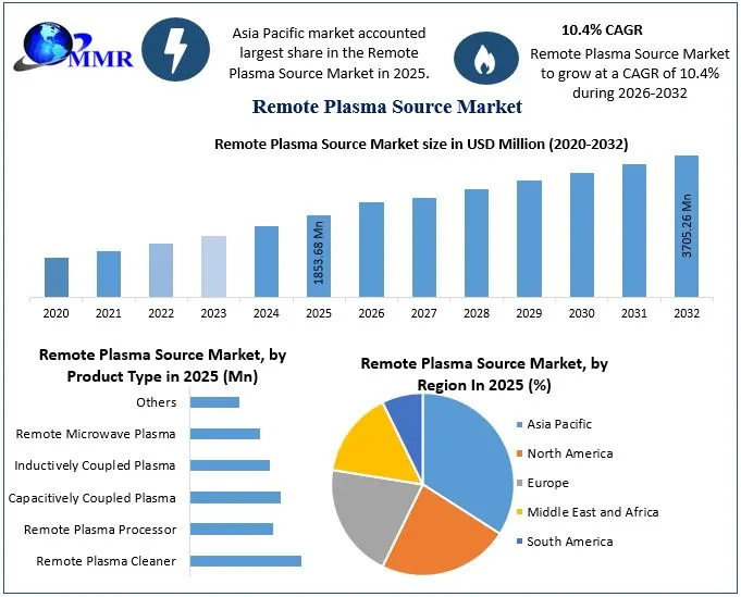 To know about the Research Methodology :- Request Free Sample Report
Remote Plasma Source Market Dynamics
Advanced Semiconductor Manufacturing to boost Remote Plasma Source Market growth
The Remote Plasma Source Market is set to experience substantial growth driven by its critical role in advancing semiconductor manufacturing processes. RPS technology is integral to the fabrication of various semiconductor products, particularly in the etching, cleaning, and deposition stages. The utilization of RPS in the creation of high-k dielectric layers, low-k dielectric layers, gallium nitride (GaN) layers, aluminum oxide layers, graphene layers, silicon nitride layers, and other semiconductor materials is a significant contributor to this market's expansion. High-k dielectric materials are pivotal in modern semiconductor devices, especially as the industry continues to push the boundaries of miniaturization. These materials are utilized as gate dielectrics in silicon-based, offering lower power consumption and improved performance in processors and memory chips.
The demand for these high-performance devices is fueling the need for precise and efficient deposition methods, such as those provided by RPS technology. Low-k dielectric materials, on the other hand, are employed in the interconnect layers of integrated circuits to reduce capacitance and improve speed. The adoption of RPS for the deposition and cleaning of these materials ensures the integrity and performance of semiconductor devices, which is crucial as the industry moves towards more advanced nodes. The growing demand for faster and more efficient electronic devices directly correlates with the increased utilization of RPS technology, driving growth in this sector.
The semiconductor industry's continuous pursuit of smaller, faster, and more efficient devices is the primary driver behind the growth of the Remote Plasma Source industry. As Remote Plasma Source manufacturers seek to overcome the challenges associated with scaling down device sizes, the precision and control offered by RPS technology become increasingly valuable. The ongoing development of new materials, such as high-k and low-k dielectrics, GaN, and graphene, is expanding the applications of RPS technology, further driving market growth. The global push towards more energy-efficient electronics, driven by both consumer demand and regulatory pressures, is enhancing the need for advanced semiconductor devices. This trend is expected to increase the adoption of RPS technology, as it plays a critical role in the production of components that enable energy efficiency, such as power semiconductors and advanced memory chips. The integration of RPS technology in semiconductor manufacturing is not only enhancing the performance of existing devices but also enabling the development of next-generation technologies.
Trends in Remote Plasma Source Market
Advancements in OLED Technology and Flexible Displays to boost Remote Plasma Source Market growth
The shift from traditional liquid crystal displays (LCDs) to more advanced organic light-emitting diode (OLED) technology is significant trend in the Remote Plasma Source industry. OLED displays, known for their superior color accuracy, contrast ratios, and energy efficiency, are pushing the boundaries of display technology. This transition is not merely a change in display type but involves a significant leap in manufacturing techniques. OLED technology demands high-precision processing due to the unique requirements of multilayer organic materials, which often necessitates the use of advanced plasma processing techniques. Remote Plasma Sources are becoming increasingly vital in this context, as they offer the precision needed to address the challenges associated with these new display materials.
A notable trend driving the RPS market is the adoption of flexible OLED displays. Unlike traditional glass-based displays, flexible OLEDs are built on heat-sensitive plastic substrates such as polyimide (PI) and polyethylene terephthalate (PET). The shift to flexible substrates introduces new challenges in plasma processing, as these materials are more delicate and susceptible to damage during manufacturing. Remote Plasma Sources are essential for performing precise plasma cleaning and etching processes required to maintain the integrity of these flexible films. The ability of RPS technology to handle these advanced materials without compromising quality is a significant factor in its growing demand. The performance of these chambers is directly linked to the cleanliness of their internal surfaces, as contaminants adversely affect film quality and lead to increased downtime. Remote Plasma Sources are particularly effective in removing contaminants from chamber walls, which is essential for sustaining high-quality production and reducing the frequency of maintenance interventions. By using RPS systems, manufacturers ensure that their equipment operates efficiently, thereby enhancing product quality and minimizing production delays.
Increased Adoption of Remote Plasma Sources in Renewable Energy
The escalating environmental concerns surrounding the semiconductor industry's use of perfluorocarbons (PFCs) are driving a significant shift towards remote plasma source technology, particularly in the realm of renewable energy. PFCs, known for their potent greenhouse gas effects, are extensively utilized in semiconductor manufacturing processes, including chamber cleaning and wafer etching. These gases, primarily nitrogen trifluoride (NF3) and other fluorinated compounds, are integral to the operation of chemical vapor deposition (CVD) reactors, where they periodically cleanse the chamber walls to remove film deposits. Chamber cleaning processes account for a substantial portion—50% to 70%—of the total PFC consumption at semiconductor fabrication sites.
| Semiconductor Product | Application | Role of RPS Technology |
| High-K Dielectric Layers | Used in transistors for advanced nodes in processors and memory chips | Enables precise deposition of high-dielectric materials for enhanced performance and reduced power consumption. |
| Low-K Dielectric Layers | Employed in interconnect layers to reduce capacitance and improve integrated circuit performance. | Facilitates the creation of low-dielectric constant layers for faster signal transmission. |
| Gallium Nitride (GaN) Layers | Used in power electronics and optoelectronic devices like LEDs and laser diodes. | Assists in producing high-quality GaN layers with low defect density, crucial for device efficiency and longevity. |
| Aluminum Oxide Layers | Commonly used as dielectric material and passivation layers in various semiconductor devices. | Ensures consistent quality and reliability of aluminum oxide layers for insulating and protective purposes. |
| Graphene Layers | Used in advanced semiconductor applications for high-performance electronics. | Aids in the deposition and patterning of graphene layers, which are known for exceptional electrical properties. |
Remote Plasma Source Market Segment Analysis
Based on Product Type, Remote Plasma Cleaner, Remote Plasma Processor, Capacitively Coupled Plasma (CCP), Inductively Coupled Plasma (ICP), Remote Microwave Plasma, and Others. Remote Plasma Cleaner segment dominated the market 2025 and is expected to hold the largest Remote Plasma Source market share over the forecast period.
The Remote Plasma Cleaner segment in the RPS market to a specialized application of remote plasma sources used for cleaning processes in various industries, particularly in semiconductor manufacturing and other high-tech industries. These cleaners use plasma generated remotely from the target surface to remove contaminants without damaging the underlying material.
Remote plasma cleaning systems generate plasma in a separate chamber from the substrate and deliver reactive species (such as radicals or ions) to the cleaning area. This allows for precise and effective removal of organic residues, thin films, and contaminants from surfaces.
Remote Plasma Source Market Recent Developments
| Date | Company | Development | Impact |
|---|---|---|---|
| 18 September 2025 | Advanced Energy Industries, Inc. | The company launched its new Opti RF power rack designed directly for legacy high-density plasma chemical vapor deposition (HDP-CVD) semiconductor equipment tools. | The system delivers over 70% system-level efficiency at full power, significantly cutting operational energy expenses and troubleshooting times for 200 mm fabs worldwide. |
| 28 November 2025 | TRUMPF SE + Co. KG | The high-tech firm officially inaugurated its new regional Technical Center for Plasma Generators in Taoyuan, Taiwan, to serve the Asian semiconductor manufacturing hub. | This facility introduces localized cleanroom capabilities to rapidly analyze, repair, and calibrate plasma units, reducing logistics complexity and lowering the carbon footprint of regional chip fabrication. |
| 11 February 2026 | MKS Instruments, Inc. | The firm integrated a series of its latest advanced power and vacuum subsystems into high-aspect-ratio plasma and reactive gas processing applications. | The technology deployment directly supported chipmakers scaling up manufacturing infrastructure to meet intensive next-generation AI server demand. |
| 13 May 2026 | MKS Instruments, Inc. | The company announced plans to open its highly automated new Super Center facility in Malaysia scheduled for completion in June 2026. | The facility expansion massively scales up corporate manufacturing capacity for vacuum, power, and plasma products to capture rising global semiconductor equipment orders. |
Remote Plasma Source Market Regional Insight
Asia Pacific dominated the market in 2025 with 38.70% and is expected to hold the largest Remote Plasma Source Market share over the forecast period. Comparing U.S. government funding for the semiconductor industry to global standards reveals significant disparities. Although the U.S. government has made substantial investments in the sector, these pale in comparison to the capital investments and market support provided by other governments. Countries in East Asia, such as South Korea, Taiwan, Japan, Malaysia, and Singapore, have implemented large-scale public investments in semiconductor fabrication, substantially boosting their global competitiveness. These regions have successfully leveraged government subsidies, tax incentives, and other forms of support to develop their semiconductor industries, which directly influences the demand for Remote Plasma Sources.
For Instance, South Korea's commitment to the semiconductor sector includes substantial financial outlays aimed at expanding its manufacturing capacity. The country's investments in research and development (R&D), coupled with tax incentives and subsidies for semiconductor facilities, have significantly enhanced its position in the global market. Similarly, Taiwan has provided extensive support to its semiconductor industry, including subsidies for land, construction, and production facilities. These investments have positioned Taiwan as a global leader in advanced semiconductor chip production, further fueling the need for advanced technologies like Remote Plasma Sources.
East Asia's dominance in the semiconductor industry, driven by substantial government support, has led to the U.S. semiconductor industry ceding certain capabilities and production activities over the years. This trend began as early as the 1980s, with U.S. companies facing increased competition from Japanese and South Korean firms benefiting from government subsidies. The U.S. industry's shift to a fabless model, where chip design occurs domestically while manufacturing is outsourced to contract manufacturers in East Asia, has further exacerbated this trend. As a result, the Remote Plasma Source Market has become increasingly reliant on demand from East Asian semiconductor manufacturers. Plurilateral trade agreements that have lowered tariffs on semiconductor-related inputs and finished products have also facilitated the expansion of the semiconductor industry in East Asia. These agreements have made it easier and more cost-effective to move wafers and chips across borders for design, production, testing, and packaging. This globalized approach has introduced efficiencies within the semiconductor industry, allowing it to keep pace with growing demand. However, it has also led to a decline in U.S.-based production and posed challenges to U.S. leadership in the industry.
Remote Plasma Source Market Competitive Landscape
October 10, 2022: Samco Unveils Plasma Enhanced ALD System for SiC and GaN Power Devices: Samco, a leading manufacturer of etching, deposition, and surface treatment processing equipment for the semiconductor and related industries and academic facilities, launches the new Plasma Enhanced Atomic Layer Deposition (PEALD) system, “AD-800LP”. The main target of the system is gate oxide film deposition for next-generation power devices of silicon carbide (SiC) and gallium nitride (GaN) materials, which will play an important role in carbon neutrality. The plasma-enhanced ALD system “AD-800LP” is a multi-purpose R&D system equipped with a unique ICP plasma source called “Tornado ICP”, in addition to the conventional thermal ALD capability. AD-800LP enables various film deposition such as oxide or nitride films by Tornado ICP, which is Samco’s proprietary plasma technology and is different from remote plasma. Tornado ICP enables stable plasma discharge even in the high-pressure range during ALD deposition.
Remote Plasma Source Market Scope: Inquiry Before Buying
| Remote Plasma Source Market | |||
|---|---|---|---|
| Report Coverage | Details | ||
| Base Year: | 2025 | Forecast Period: | 2026-2032 |
| Historical Data: | 2020 to 2025 | Market Size in 2025: | USD 1853.68 Mn |
| Forecast Period 2026 to 2032 CAGR: | 10.4% | Market Size in 2032: | USD 3705.26 Mn. |
| Segments Covered: | by Product Type | Remote Plasma Cleaner Remote Plasma Processor Capacitively Coupled Plasma (CCP) Inductively Coupled Plasma (ICP) Remote Microwave Plasma Others |
|
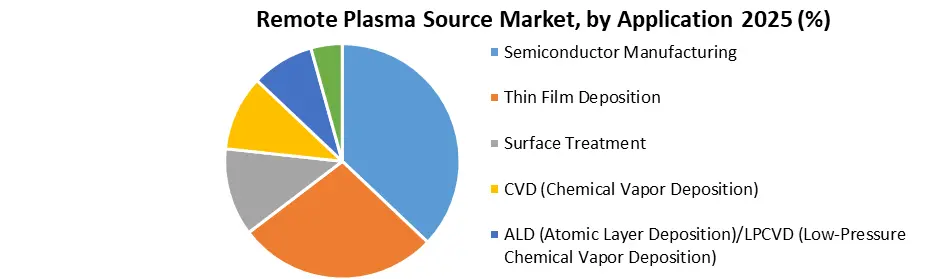
| by Application | Semiconductor Manufacturing Thin Film Deposition Surface Treatment CVD (Chemical Vapor Deposition) ALD (Atomic Layer Deposition)/LPCVD (Low-Pressure Chemical Vapor Deposition) Others |
||
Remote Plasma Source Market, by Region
North America (United States, Canada and Mexico)
Europe (UK, France, Germany, Italy, Spain, Sweden, Austria, Turkey, Russia and Rest of Europe)
Asia Pacific (China, India, Japan, South Korea, Australia, ASEAN and Rest of APAC)
Middle East and Africa (South Africa, GCC, Egypt, Nigeria and Rest of ME&A)
South America (Brazil, Argentina, Columbia and Rest of South America)
Remote Plasma Source Manufacturer
1. Advanced Energy
2. MKS Instruments, Inc.
3. MUEGGE Gerling
4. New Power Plasma
5. Oxford Instruments
6. Plasma-Therm
7. Samco Inc.
8. SENTECH Instruments GmbH
9. Tokyo Electron Ltd.
10. XEI Scientific, Inc.
11. Gencoa Ltd
12. PIE Scientific
13. SPTS Technologies Ltd.
14. Impedans Ltd
15. Chengdu Wattsine Electronic Technology
16. New Power Plasma
Frequently asked Questions:
1. What industries benefit most from Remote Plasma Sources?
Ans: Industries such as semiconductor, display (OLED), and photovoltaic sectors benefit from RPS, especially for processes like wafer cleaning, etching, and deposition.
2. How is China impacting the Remote Plasma Source market?
Ans: China's rapid advancement in the semiconductor industry, driven by government subsidies and investments, is boosting the demand for RPS in its expanding semiconductor sector.
3. What role does RPS play in OLED and flexible display production?
Ans: RPS is crucial for precise plasma cleaning and etching required for OLED and flexible display materials, especially for delicate plastic substrates used in flexible OLED displays.
4. Which regions dominate the RPS market?
Ans: Asia-Pacific leads the market, with countries like South Korea, Taiwan, and Japan investing heavily in semiconductor fabrication, further driving demand for RPS technology.
5. What is driving growth in the RPS market?
Ans: The growing demand for smaller, more efficient semiconductor devices, advancements in OLED technology, and increased focus on energy-efficient electronics are key drivers.