
Global Wafer Bonding System Market by Type, Application, Process Type, Bonding Technology, Region – Global Market Size Estimation, Industry-Wide Analysis, Competitive Landscape Assessment & Long-Term Forecast to 2032
Overview
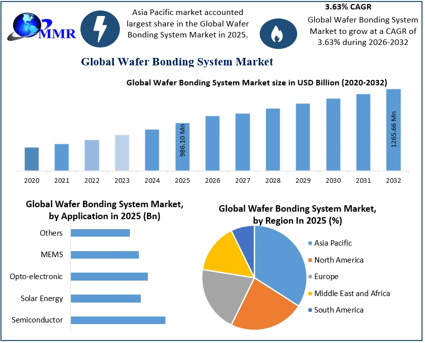
The Wafer Bonding System Market size was valued at USD 986.10 Million in 2025 and the total Wafer Bonding System revenue is expected to grow at a CAGR of 3.63% from 2025 to 2032, reaching nearly USD 1265.66 Million by 2032.
The report study has analyzed the revenue impact of COVID -19 pandemic on the sales revenue of market leaders, market followers, and market disrupters in the report, and the same is reflected in our analysis.
Wafer Bonding System Market Definition
Wafer bonding is an advanced packaging technology or process in which two wafers of any materials are bond to each other at a room temperature. It is widely used for the fabrication of NEMS, MEMS, and microelectronics and optoelectronics devices.
 To know about the Research Methodology :- Request Free Sample Report
Wafer Bonding System Market Dynamics
A surge in the adoption of wafer bonding system in microelectronics industry to produce microelectronics devices is the major driving factor behind the growth of the market. Growing market for wafers with diameter of 200nm and 300nm, rapid growth in semiconductor manufacturing and electronics industry, ongoing development in various wafer bonding methods and growing market for advanced packaging and microfluidics technology are expected to improve the growth of market during the forecast period. The wafer bonding system provides some benefits such as low bonding temperatures, high compatibility with standard CMOS wafers and insensitivity to surface topography, which are ultimately propelling the growth of the market.
However, rising need for high voltage and temperatures and high costs of wafer fabrication process are the major restraining factor that could hamper the growth of the market.
Wafer Bonding System Market Segment Analysis
By type, direct bonding segment dominated the market in 2025 and is projected to witness high growth at a CAGR of xx% during the forecast period. Direct bonding, a common type of wafer bonding process, does not require any extra intermediate layers. It is also called as fusion bonding process and it is based on the chemical bonds between two surfaces of any material. An increasing use of direct bonding process in applications such as in manufacturing of Silicon on insulator (SOI) wafers, actuators and sensors is accredited to the growth of the market.
The direct bonding process provides some benefits such as strong connection, increased compatibility, fast process, high bonding strength, high temperature stability and low cost, which is attracting various semiconductor manufacturing companies to adopt direct wafer bonding technology, which further results into growth of the market. In addition, increasing significance of direct wafer bonding process in fabrication of multi wafer micro structures such as micro pumps, micro valves, and accelerometers is expected to expand growth of the market in the coming years.
Wafer Bonding System Market Regional Insights
Region-wise, Asia Pacific held the largest market share in 2025 and is expected to maintain its dominance at a CAGR of xx% during the forecast period. The countries such as China, Japan, India, Taiwan, and South Korea are the major key contributors behind the growth of the market. The growth is attributed to the growing market for semiconductor manufacturing industry across the region.
The massive presence of various leading semiconductor manufacturing companies, increasing investments in the electronics manufacturing industries, growing market for electronic packaging industry and rising trend of smart connected devices and Internet of Things (IoT) based applications are driving growth of the market in APAC region.
The objective of the report is to present a comprehensive analysis of the Global Wafer Bonding System Market including all the stakeholders of the industry. The past and current status of the industry with forecasted market size and trends are presented in the report with the analysis of complicated data in simple language.
The report covers all the aspects of the industry with a dedicated study of key players that includes market leaders, followers and new entrants. PORTER, SVOR, PESTEL analysis with the potential impact of micro-economic factors of the market has been presented in the report. External as well as internal factors that are supposed to affect the business positively or negatively have been analyzed, which will give a clear futuristic view of the industry to the decision-makers.
The report also helps in understanding Global Wafer Bonding System Market dynamics, structure by analyzing the market segments and projects the Global Wafer Bonding System Market. Clear representation of competitive analysis of key players by Application, price, financial position, Product portfolio, growth strategies, and regional presence in the Global Wafer Bonding System Market make the report investor’s guide.
Wafer Bonding System Market Scope: Inquire before buying
| Global Wafer Bonding System Market | |||
|---|---|---|---|
| Report Coverage | Details | ||
| Base Year: | 2025 | Forecast Period: | 2026-2032 |
| Historical Data: | 2020 to 2025 | Market Size in 2025: | USD 986.10 Mn. |
| Forecast Period 2026 to 2032 CAGR: | 3.63% | Market Size in 2032: | USD 1265.66 Mn. |
| Segments Covered: | by Type | Direct Bonding Anodic Bonding Solder/Eutectic/ Diffusion Bonding Glass-Frit Bonding Adhesive Bonding Others |
|
| by Application | Semiconductor Solar Energy Opto-electronic MEMS Others |
||
| by Process Type | Die To Die Bonding Die To Wafer Bonding Wafer To Wafer Bonding |
||
| by Bonding Technology | Die Bonding Technology Wafer Bonding Technology Wafer Bonding Technology Direct and Anodic Wafer Bonding Indirect Wafer Bonding |
||
Wafer Bonding System Market, by Region
North America (United States, Canada and Mexico)
Europe (UK, France, Germany, Italy, Spain, Sweden, Austria and Rest of Europe)
Asia Pacific (China, South Korea, Japan, India, Australia, Indonesia, Malaysia, Vietnam, Taiwan, Bangladesh, Pakistan and Rest of APAC)
Middle East and Africa (South Africa, GCC, Egypt, Nigeria and Rest of ME&A)
South America (Brazil, Argentina Rest of South America)
Wafer Bonding System Market, Key Players are
1. 3M
2. Applied Microengineering
3. Ayumi Industry
4. Dynatex International
5. EV Group
6. NxQ
7. Palomar Technologies
8. SüSS Microtec SE
9. Tokyo Electron
10. Micronit Microtechnologies
11. Mitsubishi Heavy Industries Machine Tool Co., Ltd.
12. Coral Foodstuff Machine Co., Ltd
13. Komachine.com, Co
14. Thermo Electric Company, Inc.
15. Logitech LTD
16. Electron-Mec s.r.l
17. Inseto
Frequently Asked Questions:
1. Which region has the largest share in Global Market?
Ans: Asia Pacific region held the highest share in 2025.
2. What is the growth rate of Global Market?
Ans: The Global Market is growing at a CAGR of 3.63% during forecasting period 2026-2032.
3. What is scope of the Global Market report?
Ans: Global Market report helps with the PESTEL, PORTER, COVID-19 Impact analysis, Recommendations for Investors & Leaders, and market estimation of the forecast period.
4. Who are the key players in Global Market?
Ans: The important key players in the Global Market are – 3M, Applied Microengineering, Ayumi Industry, Dynatex International, EV Group, NxQ, Palomar Technologies, SüSS Microtec SE, Tokyo Electron, Micronit Microtechnologies, Mitsubishi Heavy Industries Machine Tool Co., Ltd., Coral Foodstuff Machine Co., Ltd, Komachine.com, Co, Thermo Electric Company, Inc., Logitech LTD, Electron-Mec s.r.l, and Inseto.
5. What is the study period of this Market?
Ans: The Global Market is studied from 2025 to 2032.