
Thin Wafer Processing and Dicing Equipment Market Size – Industry Structure Evaluation, Demand Drivers Analysis, Regional Growth Analysis and Identification, Competitive Positioning Review & Global Market Size Forecast to 2032
Overview
The Thin Wafer Processing and Dicing Equipment Market size was valued at USD 682.30 Billion in 2024 and the total Thin Wafer Processing and Dicing Equipment revenue is expected to grow at a CAGR of 6.5% from 2025 to 2032, reaching nearly USD 1129.21 Billion.
Thin wafer processing equipment fabricates ultra-thin semiconductor wafers for flexible and high-performance applications, while dicing equipment precisely separates integrated circuits from wafers, ensuring accuracy in electronic component production. The increasing demand for miniaturized electronic devices across various industries such as consumer electronics, automotive, and healthcare driving the growth of The Thin Wafer Processing and Dicing Equipment Market. The market growth scenario reflects a rising emphasis on thin wafer processing equipment to fabricate semiconductor wafers with reduced thickness, enabling advancements in flexibility, performance, and miniaturization. While, dicing equipment plays a major role in semiconductor manufacturing, ensuring precise separation of integrated circuits from wafers to meet stringent quality and reliability standards.
The Thin Wafer Processing and Dicing Equipment Market Key growth factors include technological advancements in equipment design, such as laser-based dicing systems and advanced thinning techniques, coupled with the expanding semiconductor industry's footprint in emerging economies. The growing adoption of 5G technology, artificial intelligence, and Internet of Things (IoT) devices is boosting demand for thin wafer processing and dicing equipment to support the production of high-performance chips. Recent developments by The Thin Wafer Processing and Dicing Equipment Market key players include strategic collaborations, product launches, and investments in research and development to enhance equipment efficiency, throughput, and precision.
For instance, companies such as Disco Corporation, Tokyo Electron Limited, and Applied Materials Inc. have introduced innovative solutions focused on improving wafer thinning and dicing processes, addressing the evolving needs of semiconductor manufacturers worldwide. These advancements aim to fulfil to the increasing demand for advanced semiconductor devices while maintaining high levels of productivity and yield, driving the growth trajectory of the thin wafer processing and dicing equipment market in the forecast period.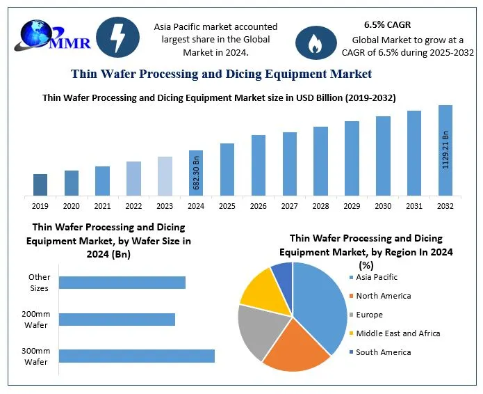 To know about the Research Methodology :- Request Free Sample Report
Thin Wafer Processing and Dicing Equipment Market Dynamics:
Increasing Demand for Miniaturized Electronic Devices Driving Thin Wafer Processing and Dicing Equipment Market Growth
The demand for thin wafer processing and dicing equipment is driven by the increasing need for thinned wafers driven by consumer applications such as smartphones, smart cards, and stacked packages. The market for thinned wafers, used in various applications including MEMS devices, CMOS Image Sensors, memory, logic devices, and power devices, is estimated to have exceeded 16.5 million 8-inch wafer starts per year (WSPY) in 2025 and is expected to reach nearly 32 million 8-inch WSPY by 2032, representing a compound annual growth rate (CAGR) of 14%. Thinner wafers offer several benefits, including enabling thin packaging with improved form factors, enhanced electrical performance, and superior heat dissipation.
The growth in the thin wafer processing and dicing equipment market is boosted by technological advancements such as the TAIKO process developed by DISCO for backside metallization layer in power devices. This innovative thinning process has already entered mass production, fulfiling to the evolving needs of manufacturers like Infineon and STMicroelectronics. The evolution of dicing technology is driven by the demand for thinner wafers and stronger die, with mechanical dicing being the most common method, supplemented by alternative technologies such as stealth dicing and plasma dicing based on deep reactive ion etching technology.
The dicing equipment market, is expected to double by . Companies such as DISCO lead in blade dicing products, while Accretech dominates in stealth dicing. However, emerging players like Plasma-Therm, Orbotech/SPTS, and Panasonic are challenging the landscape with plasma dicing tools, offering promising alternatives for semiconductor manufacturers. This comprehensive overview of dicing technologies and equipment benchmarks their features, applications, and competitive landscape, providing valuable insights for stakeholders in the thin wafer processing and dicing equipment market.
Complexity in MEMS and Advanced Packaging Hinders the Thin Wafer Processing and Dicing Equipment Market Growth
Rising demand for higher memory densities and functionality, the industry faces mounting pressure to meet reliability, manufacturability, cost, and yield requirements have challenges such as particularly in packaging where wafer thinning and dicing processes encounter hurdles and hinders the growth of Thin Wafer Processing and Dicing Equipment Market. Challenges arise from thin film stresses within wafers during memory cell fabrication, leading to complications in wafer preparation and assembly. While mechanical dicing is conventional, it introduces issues like chipping and reduced die strength, necessitating alternative methods such as laser ablation and stealth dicing. Yet, adopting these alternatives adds complexity and cost, thereby impacting overall production efficiency and yield, highlighting a major hurdle in the Thin Wafer Processing and Dicing Equipment Market growth.
Handling thin and fragile memory die during the die attach process poses additional challenges, demanding specialized tools and techniques to minimize stress and prevent die cracking. The necessity for automatic optical inspection to detect post-die attach cracks further complicates processes, adding layers of complexity and cost. The emergence of integrated devices such as solid-state drives (SSDs) and consumer system-in-package (SiP) modules introduces unique challenges for package design and assembly. These challenges include the demand for higher stacking and reduced space for wire bond fingers and passive components, driving the need for thin substrates capable of supporting increased routing. Consequently, the market grapples with heightened complexity in packaging design and assembly, underscoring the urgent need for innovative solutions to ensure high reliability, manufacturability, and yield while addressing evolving semiconductor application demands.
Thin Wafer Processing and Dicing Equipment Market Segment Analysis:
Based on Type of Wafer Material, Silicon wafers dominated the market in Thin Wafer Processing and Dicing Equipment Market in 2024 due to their extensive use in traditional semiconductor devices such as integrated circuits (ICs), MEMS devices, and CMOS image sensors. The widespread adoption of silicon wafers is driven by their superior electrical properties, reliability, and cost-effectiveness. In contrast, compound semiconductor wafers, including materials like gallium arsenide (GaAs) and silicon carbide (SiC), find niche applications in high-frequency and power electronics, optoelectronics, and RF devices due to their superior performance in specific applications requiring high-speed operation and high-temperature resistance. Glass wafers, while less common, are gaining traction in emerging applications such as microfluidics, bioMEMS, and optical devices due to their excellent optical transparency, chemical inertness, and biocompatibility, offering unique advantages in specialized areas such as biomedical and optical industries.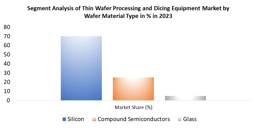
Thin Wafer Processing and Dicing Equipment Market Regional Insights:
Asia Pacific Dominates the Thin Wafer Processing and Dicing Equipment Market
Asia Pacific dominated the Thin Wafer Processing and Dicing Equipment Market in 2024 as it is most rapidly growing semiconductor market globally, driven by robust demand for smartphones and consumer electronics devices, particularly in countries like China, South Korea, and Singapore. The region's prominence is evident in strategic business moves, such as Wingtech's acquisition of Newport Wafer Fab in August , underscoring China's focus on expanding through mergers and acquisitions.
Japan, with its strong semiconductor and electronics industry, plays a pivotal role, although it faces challenges such as high production costs and exchange rate fluctuations. In contrast, Australia experiences market growth propelled by a flourishing electronics manufacturing sector and increased adoption of advanced devices, particularly in televisions and smartphones. In a bid to bolster semiconductor supply chain security, the Quad Alliance, comprising Australia, India, the United States, and Japan, initiated a semiconductor supply chain initiative in October .
India, currently reliant on semiconductor imports, unveiled a comprehensive program in December to develop its semiconductor and display manufacturing ecosystem, aiming for economic independence and technological leadership. The Asia Pacific region significantly influences the growth trajectory of fully autonomous automobiles, driven by technological advancements, consumer acceptance, pricing, and OEMs' capacity to address safety concerns. This dynamic landscape underscores continuous efforts by the automotive and semiconductor industries to enhance technologies and ensure reliable integration of autonomous features into vehicles.
Thin Wafer Processing and Dicing Equipment Market Scope: Inquire before buying
| Global Thin Wafer Processing and Dicing Equipment Market | |||
|---|---|---|---|
| Report Coverage | Details | ||
| Base Year: | 2024 | Forecast Period: | 2025-2032 |
| Historical Data: | 2019 to 2024 | Market Size in 2024: | USD 682.30 Bn. |
| Forecast Period 2025 to 2032 CAGR: | 6.5% | Market Size in 2032: | USD 1129.21 Bn. |
| Segments Covered: | by Type of Wafer Material | Silicon Compound Semiconductors Glass |
|
| by Technology Type | Dicing Equipment Thin Wafer Processing Equipment |
||
| by Wafer Size | 300mm Wafer 200mm Wafer Other Sizes |
||
| by Application | MEMS (Micro-Electro-Mechanical Systems) CMOS Image Sensors RF Devices Memory Devices Logic and Power Devices |
||
| by End-User | Semiconductor Manufacturing Electronics Automotive Healthcare Aerospace Industries) |
||
Thin Wafer Processing and Dicing Equipment Market, By Region
North America (United States, Canada and Mexico)
Europe (UK, France, Germany, Italy, Spain, Sweden, Austria and Rest of Europe)
Asia Pacific (China, South Korea, Japan, India, Australia, Indonesia, Malaysia, Vietnam, Taiwan, Bangladesh, Pakistan and Rest of APAC)
Middle East and Africa (South Africa, GCC, Egypt, Nigeria and Rest of ME&A)
South America (Brazil, Argentina Rest of South America)
Thin Wafer Processing and Dicing Equipment Market Key Players
North America:
1. Dynatex International, Petaluma, California, United States
2. Modutek Corporation, San Jose, California, United States
3. Technotronix Corporation, San Jose, California, United States
4. Axus Technology, Chandler, Arizona, United States
5. Plasma-Therm LLC, Saint Petersburg, Florida, United States
Europe:
1. Advanced Dicing Technologies Ltd., Yokneam, Israel
2. Loadpoint Ltd., Rye, United Kingdom
3. SUSS MicroTec SE, Garching, Germany
4. Microdiamant AG, Lengwil, Switzerland
5. Meyer Burger Technology AG, Thun, Switzerland
Asia-Pacific:
1. Disco Corporation, Tokyo, Japan
2. Accretech, Tokyo, Japan
3. Hanmi Semiconductor Co., Ltd., Chungcheongbuk-do, South Korea
4. Nagase Integrex Co., Ltd., Tokyo, Japan
5. Tokyo Seimitsu Co., Ltd., Tokyo, Japan
FAQs:
1] What Major Key players in the Global Thin Wafer Processing and Dicing Equipment Market report?
Ans. The Major Key players covered in the Market report are Disco Corporation,Accretech,Hanmi Semiconductor Co., Ltd., Nagase Integrex Co., Ltd.,Tokyo Seimitsu Co., Ltd. Navenio,Huq Industries Limited,Cambium Networks Ltd,Purple,OpenSignal,Relayr,Briteyellow,WiCastr
2] Which region is expected to hold the highest share in the Global Thin Wafer Processing and Dicing Equipment Market?
Ans. Asia Pacific region is expected to hold the highest share in the Market.
3] What is the market size of the Global Market by 2032?
Ans. The market size of the Market by 2032 is expected to reach USD 1129.21 Billion.
4] What is the forecast period for the Global Market?
Ans. The forecast period for the Market is 2025-2032.
5] What was the Global Thin Wafer Processing and Dicing Equipment Market size in 2024?
Ans: The Global Thin Wafer Processing and Dicing Equipment Market size was USD 682.30 Billion in 2024.