
Semiconductor Etch Equipment Market Size by Type, Process, Application, Region – Segment-Level Market Assessment, Growth Opportunity Analysis, Competitive Mapping & Forecast to 2032
Overview
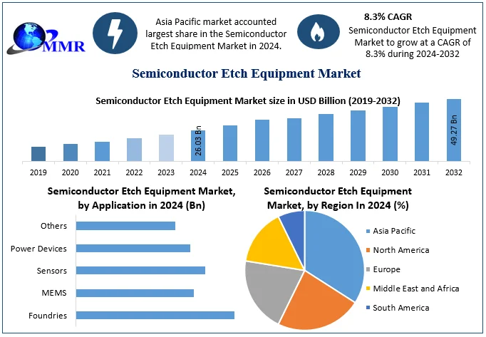
Semiconductor Etch Equipment Market was valued at USD 26.03 Bn in 2024 and is expected to reach USD 49.27 Bn by 2032, at a CAGR of 8.3 % during the forecast period.
Semiconductor Etch Equipment Market Overview
Semiconductor etch equipment is a device used to remove selective materials from the surface of the silicon wafer substrate by using various chemicals. The etching process removes the material from the surface of the semiconductor to create patterns according to its applications. Semiconductor etch equipment are used to remove layers from the silicon wafer surface through application of various chemicals. The demand for semiconductor etch equipment is increasing significantly as a result of continuously increasing precision requirement of semiconductor devices.
In semiconductor device fabrication, etching is technology that selectively remove material from a thin film on a substrate (with or without prior structures on its surface) and by this removal create a pattern of that material on the substrate.
As Semiconductor Etch Equipment manufacturing trend towards low volume diversified production continue to advance, semiconductor etch equipment suppliers witness consistent demand from buyers looking to maintain optimum processing conditions in response to variations in equipment and products.
 To know about the Research Methodology :- Request Free Sample Report
The semiconductor etch equipment market is a key sector within the broader semiconductor manufacturing industry. Technological advancements play a significant role in shaping the semiconductor etch equipment market. Key trends include the development of advanced etching techniques such as plasma etching, dry etching, and chemical etching, as well as the integration of process control and automation features to enhance precision and throughput.
Semiconductor Etch Equipment Market Dynamics
Rapid growth of the semiconductor industry to boost Semiconductor Etch Equipment Market growth
Semiconductor manufacturing, vital to modern technology, relies on a specialized ecosystem of capital goods and tools, from advanced lithography systems to precise etching tools. These machines work seamlessly across fabrication stages, producing accurate microchips. The ecosystem includes cleaning systems, wafer handling robots, and cleanroom infrastructure to maintain pristine conditions. The Government of India's Scheme for Promotion of Manufacturing of Electronic Components and Semiconductors (SPECS) is designed to boost domestic manufacturing and attract substantial investments across the entire electronics value chain.
The Indian government is actively fostering the growth of the semiconductor etch equipment market, aiming to boost India into a prominent global position in the electronics sector. Through the facilitation of manufacturing facilities dedicated to electronics, semiconductors, and displays, India is laying the groundwork to become a key player in achieving the government's ambitious target of generating USD 1 trillion in economic value from the nation's digital economy by 2025.
The increasing usage of Etch Equipment in automotive sector to boost the Semiconductor Etch Equipment Market growth
In modern automobiles, semiconductor devices play a crucial role in various critical functions such as sensing, safety features, displays, vehicle control, and power management. Particularly in electric and hybrid vehicles (EVs), the utilization of semiconductors is expanding significantly. These semiconductor devices facilitate the implementation of safety systems and semi-autonomous driver assistance features. They enable smart functionalities including blind-spot detection systems, backup cameras, collision-avoidance sensors, adaptive cruise control, lane-change assist, airbag deployment sensors, and emergency braking systems. The integration of semiconductors in automotive applications significantly boosts the Semiconductor Etch Equipment Market growth.
Trade Uncertainties to restraint Semiconductor Etch Equipment Market growth
The electronics industry faces repercussions from the US-Chinese trade war and broader global political instability. The slowdown in semiconductor industry conditions correlates with global economic uncertainty, largely influenced by the ongoing trade tensions between China and the US, alongside the deceleration of the Chinese economy.
Semiconductors, being crucial components with intricate manufacturing processes, form a highly traded commodity. Excessively convoluted customs and trade regulations, procedures, and norms have the potential to significantly disrupt semiconductor supply chains, leading to costly impediments that detrimentally affect both consumers and businesses. These factors act as restraints for Semiconductor Etch Equipment Market growth.
The shortage of raw material to limit the Semiconductor Etch Equipment Market growth
In an unparalleled economic environment, manufacturers across all sectors faced challenges in meeting supply and demand. The chip making industry experienced prolonged production halts during the pandemic due to government-imposed shutdowns and restrictions. Upon resuming production, semiconductor companies encountered heightened pressure from multiple sectors. Shortages of raw materials and disruptions in semiconductor production caused by various natural and other factors impacted the semiconductor industry, thereby constraining growth in the semiconductor etch equipment market.
Semiconductor Etch Equipment Market Segment Analysis
Based on Process, the market is segmented into Dielectric Etch, Conductor Etch, and Other. Conductor Etch segment dominated the market in 2024 and is expected to hold the largest Semiconductor Etch Equipment Market share over the forecast period. Conductor etching equipment is widely employed to sculpt electrically activated materials found in diverse semiconductor device components. Even minor deviations in these intricate semiconductor structures can lead to electrical flaws that undermine the device's functionality. The designs for conductor etching are so minute that the etching process often stretches the limits of standard wafer sizes. Moreover, conductor etching involves the application of electromagnetic combustion energy to a gas containing a chemically reactive element such as fluorine. The expansion of the Conductor Etching Systems market is heavily contingent upon the progress of the broader semiconductor equipment market on a global scale.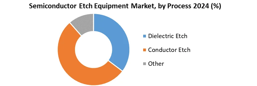
Semiconductor Etch Equipment Market Regional Insight
Growing investments in Semiconductor Manufacturing to boost Asia Pacific Semiconductor Etch Equipment Market growth
The Asia-Pacific region has the most prominent share of global semiconductor foundries, with major companies such as TSMC, Samsung Electronics, etc. Taiwan, South Korea, Japan, and China have a significant market share in the region. US chipmaker Micron is setting up a new semiconductor assembly and test facility in Gujarat, contributing to the region's growing importance in the industry. Another semiconductor fabrication unit, display fabrication unit be commenced in near future which increase demand for semiconductor capital equipment & tools.
China, Japan, Malaysia, Singapore, Vietnam, South Korea, etc. were the largest exporters of Semiconductor Manufacturing Equipment. China is the largest importer and exporter of semiconductor devices including Semiconductor Etch Equipment Market. The concentrated supply of SME from these five countries reflects the overall consolidation and competitiveness of firms engaged in the Semiconductor Etch Equipment industry.
As the next section shows, the industry is increasingly mature, with a small number of large firms controlling nearly two-thirds of global Semiconductor Etch Equipment market share. Semiconductor Etch Equipment export in China/Taiwan is increasing day by day due to large manufacturing facility in the region. The demand for SME in Asia reflects a broader trend in the industry; as semiconductors have become more intensively produced and consumed in Asia, the SME industry’s supply chain has changed accordingly to meet this increase in demand. China’s ambitious plans for the development of its domestic semiconductor industry has fundamentally shifted demand for SME.

According to a survey conducted by the Semiconductor Industry Association in July 2021, China mastered several chip technologies, and its commercial semiconductor industry is still relatively young. Still, the Chinese government is trying to close the gap, investing more than USD 150 billion in semiconductors between 2014 and 2030. Supported by booming markets and these government investments, China is poised to become increasingly competitive in some semiconductor market segments.
According to a December 2022 report from CNBC, China is in the process of developing a support package exceeding CNY 1 trillion (USD 143 billion) for its semiconductor industry. This initiative represents a significant stride towards achieving self-reliance in chip manufacturing and serves as a response to efforts by the United States aimed at impeding China's technological progress, which significantly boost the Asia Pacific Semiconductor Etch Equipment Market growth. Beijing intends to implement one of its most substantial fiscal stimulus packages over a five-year period, primarily consisting of subsidies and tax credits. These incentives are designed to bolster domestic semiconductor production and research endeavors.
Japan's government is offering financial aid to encourage foreign chip makers to build plants in Japan, which is creating a positive growth outlook for the market. For instance, in June 2022, Japan's Ministry of Economy, Trade and Industry (METI) announced plans to offer subsidies worth up to JPY 476 billion (USD 3.5 billion) for a semiconductor plant being built in Kumamoto Prefecture by Taiwan Semiconductor Manufacturing Co. (TSMC), Sony Group and Denso. Total investment in the plant was expected to reach around USD 8.6 billion, with Japan's government supporting about 40% of the costs.
A similar trend has also been observed across other countries in the region.
For instance, in February 2022, Lam Research, a US semiconductor equipment company, manufactured next-generation core equipment for semiconductor manufacturing in South Korea. These highly selective etching devices support Gate All Around (GAA) and 3D stacking technology. The new equipment is expected to play an important role in developing Samsung Electronics' next-generation memory and system semiconductors.
March 26, 2024: Lam Research Corp. introduced the world's first production-oriented pulsed laser deposition (PLD) tool to enable next-generation MEMS-based microphones and radio frequency (RF) filters. Lam's Pulsus PLD system delivers aluminum scandium nitride (AlScN) films with the highest scandium content available. This paves the way for advanced consumer and automotive devices with enhanced performance, capability and functionality. Pulsus is now shipping to select specialty device manufacturers. The addition of Pulsus PLD to the Lam portfolio further expands Lam's comprehensive range of deposition, etch and single-wafer clean products focused on specialty technologies and demonstrates Lam's continuous innovation in this sector.
April 18, 2023: Hitachi High-Tech Corporation ("Hitachi High-Tech") announced that they are going to construct a new production facility in Kasado Area of Kudamatsu City, Yamaguchi Prefecture, with a view to increasing production capacity of etching systems for its semiconductor manufacturing equipment business, with production scheduled to begin in FY2025. The new facility will double production capacity through digitalized and automated production lines, in order to cater to the ever-increasing demand for semiconductor manufacturing equipment.
In June 2022, AlixLab developed a new, innovative method for manufacturing semiconductor components with a high degree of packing, eliminating several steps in the manufacturing process - Atomic Layer Etch Pitch Splitting (APS). According to the company, the method makes the components cheaper and less resource-intensive. The company also announced the completion of the Atomic Layer Etch (ALE) equipment hook-up in its clean room at ProNano RISE in Lund, Sweden.
Strategic Recommendations for Stakeholders
The semiconductor industry stakeholders should consider the following strategic recommendations in order to capitalize on opportunities and overcome obstacles.
R&D investments: Continued investments in semiconductor R&D are essential to drive innovation, enhance manufacturing processes, and develop future-ready technologies.
Collaboration and partnerships: Collaboration throughout the semiconductor ecosystem, including manufacturers, equipment suppliers, and research institutions, foster knowledge exchange, drive technological advancements, and collectively address complex challenges.
Acquisition and talent development: The semiconductor industry requires a skilled workforce to drive innovation. Through educational programs, internships, and training initiatives, stakeholders seek to attract and cultivate talent, which is expected to boost the Semiconductor Etch Equipment Market growth.
Sustainability: Adopting sustainable practices in the manufacturing and operations of semiconductors can reduce environmental impact, improve energy efficiency, and contribute to a greener future. Businesses prioritize sustainability initiatives and develop eco-friendly solutions.
The Scope of Global Semiconductor Etch Equipment Market: Inquire before buying
| Global Semiconductor Etch Equipment Market | |||
|---|---|---|---|
| Report Coverage | Details | ||
| Base Year: | 2024 | Forecast Period: | 2025-2032 |
| Historical Data: | 2019 to 2024 | Market Size in 2024: | USD 26.03 Bn. |
| Forecast Period 2025 to 2032 CAGR: | 8.3% | Market Size in 2032: | USD 49.27 Bn. |
| Segments Covered: | by Type | Wet etch equipment Dry etch equipment |
|
| by Process | Dielectric Etch Conductor Etch Other |
||
| by Application | Foundries MEMS Sensors Power Devices Others |
||
Semiconductor Etch Equipment Market, by Region
North America (United States, Canada and Mexico)
Europe (UK, France, Germany, Italy, Spain, Sweden, Austria and Rest of Europe)
Asia Pacific (China, South Korea, Japan, India, Australia, Indonesia, Malaysia, Vietnam, Taiwan, Bangladesh, Pakistan and Rest of APAC)
Middle East and Africa (South Africa, GCC, Egypt, Nigeria and Rest of ME&A)
South America (Brazil, Argentina Rest of South America)
Leading Semiconductor Etch Equipment manufacturers includes:
North America Leading Semiconductor Etch Equipment manufacturers include:
1. Lam Research (USA)
2. Applied Materials (USA)
3. KLA Corporation (USA)
4. Plasma-Therm (USA)
5. MKS Instruments (Andover, Massachusetts, United States)
6. Rogue Valley Microdevices, Inc. (Medford, Oregon, USA)
7. ASML (The Netherlands)
Asia Pacific Semiconductor Etch Equipment key players include:
8. SCREEN Holdings Co., Ltd (Japan)
9. Tokyo Electron Ltd. (Japan)
10. Hitachi Ltd. (Japan)
11. Samco Inc. (Kyoto, Japan)
12. NAURA Technology Group Co., Ltd. (Beijing, China)
13. GigaLane Co., Ltd. (Hsinchu, Taiwan)
14. SAMCO (Kyoto, Japan)
15. Gigalane (Hwaseong, South Korea)
16. Panasonic Corporation (Kadoma, Osaka, Japan)
17. Advanced Micro-Fabrication Equipment Inc. (China)
18. SHINKO SEIKI CO., LTD. (Japan)
19. ULVAC, Inc (Japan)
Europe Semiconductor Etch Equipment manufacturer include:
20. Corial SAS (Bernin, France)
21. Diener Electronic (Baden-Württemberg, Germany)
22. Oxford Instruments plc (Abingdon, United Kingdom)
23. SPTS Technologies Ltd. (Newport, United Kingdom)
Frequently asked Questions:
1. What is semiconductor etch equipment?
Ans: Semiconductor etch equipment is used to remove selective materials from the surface of silicon wafer substrates using various chemicals. It helps create patterns on semiconductor surfaces according to specific applications.
2. What are the key trends in semiconductor etch equipment?
Ans: Key trends include the development of advanced etching techniques such as plasma etching, dry etching, and chemical etching, along with the integration of process control and automation features to enhance precision and throughput.
3. What are the factors restraining the growth of the semiconductor etch equipment market?
Ans: Trade uncertainties, including those stemming from the US-China trade war, and shortages of raw materials are significant factors restraining the growth of the semiconductor etch equipment market.
4. How does Asia Pacific contribute to the growth of the semiconductor etch equipment market?
Ans: Growing investments in semiconductor manufacturing in the Asia-Pacific region, particularly in countries like Taiwan, South Korea, Japan, and China, are driving the growth of the semiconductor etch equipment market.