Atomic Layer Deposition Market Size by Product, Type, Application, End-User, Region, Industry-Wide Analysis, Competitive Landscape Assessment & Long-Term Forecast to 2032

13.14%
CAGR (2026-2032)
2.28 USD Bn.
Market Size
326
Report Pages
150
Market Tables

Overview

Atomic Layer Deposition Market was valued US$ 2.28 Bn in 2025 and is expected to reach US$ 5.41 Bn by 2032 and will grow at a 13.14% CAGR during the forecast period.

The report includes the analysis of impact of COVID-19 lock-down on the revenue of market leaders, followers, and disrupters. Since lock down was implemented differently in different regions and countries, impact of same is also different by regions and segments. The report has covered the current short term and long term impact on the market, same will help decision makers to prepare the outline for short term and long term strategies for companies by region.Atomic Layer Deposition Market Snapshot

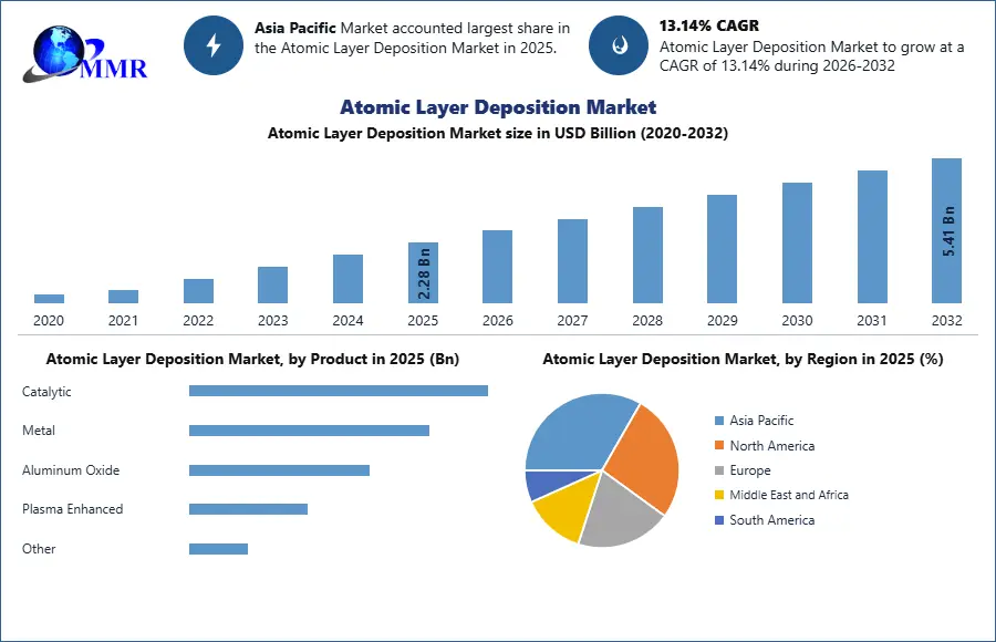
To know about the Research Methodology:-Request Free Sample Report

Increasing demand from end use industries like automotive, industrial, and medical sectors drives the atomic layer deposition market. Growing application of atomic layer deposition in nanotechnology and 3D NAND memory systems is further accelerating the growth of atomic layer deposition market. Application of atomic layer deposition in power devices, energy storage systems, hydrophobic coatings, flexible electronics, and electronic textiles provide several growth opportunities for the atomic layer deposition market. However, high cost of initial investment and stringent export procedures and policies act as a barrier for the market. At present, market is experiencing scarcity of skilled professionals thereby posing a challenge for market.

Solar device & medical equipment segment are the two fastest-growing applications for the atomic layer deposition market owing to the growth of each industry globally. Semiconductor & electronics segment dominated the market with 68% in 2023. Atomic layer deposition is used in IC (Integrated Circuit) and Non-IC components for miniaturizing device’s dimension and generate high durability which influences the growth of the semiconductor & electronics market.

Aluminum oxide segment is dominating the atomic layer deposition (ALD) market. Plenty availability of aluminum, exceptional properties offerings, stability to numerous substrates, easy accessibility of precursor material and economic base metal prices, has resulted into increased demand for aluminum oxide. While, plasma enhanced- atomic layer deposition is expected to be the fastest growing product type. Plasma enhanced- atomic layer deposition delivers excellent output properties and fastest surface reaction mechanism rate. Atomic layer deposition is surface-sensitive deposition process, and enhances the surface modification through plasma exposure, which enables to alter nucleation.

Asia Pacific held 46% of the overall revenue in 2023 owing to strong presence of manufacturing base and growing semiconductor & electronics, solar, and medical device industries, especially, in China, Japan, South Korea, and Taiwan. Presence of cheap skilled labor & land, and government subsidies further accelerate the market growth. Europe and North America are mature market hence is anticipated to grow at steady pace. North America accounted for the second largest market share of 23.8% in 2023, driven by technological advancement and growing application of atomic layer deposition equipment across automotive, semiconductor, and industrial sectors, among others.

The objective of the report is to present a comprehensive assessment of the market and contains thoughtful insights, facts, historical data, industry-validated market data and projections with a suitable set of assumptions and methodology.

The report also helps in understanding atomic layer deposition market dynamics, structure by identifying and analyzing the market segments and project the market size. Further, the report also focuses on a competitive analysis of key players by product, price, financial position, product portfolio, growth strategies, and regional presence.

The report also provides PEST analysis, PORTER's analysis, SWOT analysis to address questions of shareholders to prioritizing the efforts and investment in the near future to the emerging segment in atomic layer deposition market.

Scope of Global Atomic Layer Deposition Market: Inquire before buying

Atomic Layer Deposition Market
Report Coverage Details
Base Year: 2025 Forecast Period: 2026-2032
Historical Data: 2020 to 2025 Market Size in 2025: 2.28 USD Billion
Forecast Period 2026-2032 CAGR: 13.14% Market Size in 2032: 5.41 USD Billion
Segments Covered: by Product Catalytic
Metal
Aluminum Oxide
Plasma Enhanced
Other
by Type Film Type
Precursor Type
Material Type
Polymers
Sulfides
Nitrides
Oxides
Other
by Application Medical Devices
Optical Devices
Sensors
Solar Panels & Devices
Thermoelectric Materials
Integrated Circuit Applications
Fuel Cells
Batteries
Other
by End-User Healthcare
Chemicals
Energy
Semiconductors & Electronics
Other

Atomic Layer Deposition Market, by Region:

North America (United States, Canada and Mexico)
Europe (UK, France, Germany, Italy, Spain, Sweden, Austria and Rest of Europe)
Asia Pacific (China, South Korea, Japan, India, Australia, Indonesia, Malaysia, Vietnam, Taiwan, Bangladesh, Pakistan and Rest of APAC)
Middle East and Africa (South Africa, GCC, Egypt, Nigeria and Rest of ME&A)
South America (Brazil, Argentina Rest of South America)

Atomic Layer Deposition Market, Key Players are:

01.AIXTRON SE
02.Adeka Corporation
03.Air Liquide S.A.
04.Air Products and Chemicals, Inc
05.Applied Materials, Inc.
06.Adeka Corp
07.Applied Materials Inc
08.ASM International N.V
09.ATMI Inc
10.Beneq Oy
11.Cambridge NanoTech Inc
12.Hitachi Kokusai Electric Inc
13.Kurt J. Lesker Co
14.Metryx Ltd
15.Novellus Systems Inc
16.Oxford Instruments plc
17.Picosun Oy
18.Praxair Technology Inc
19.Sigma-Aldrich Co.
20.Lam Research Corporation
21.Tokyo Electron Limited
22.Denton Vacuum
23.Kurt J. Lesker Company
24.Veeco Instruments.
25.Ultratech Inc.
26.Centrotherm Photovoltaics AG
27.Tosoh Corporation

Frequently Asked questions

1. What is the market size of the Global Atomic Layer Deposition Market in 2025?
Ans. The market size Global market in 2025 was US$ 2.28 Billion.

2. What are the different segments of the Global Atomic Layer Deposition Market?
Ans. The Global market  is divided into Product, Type, Application and End-User.

3. What is the study period of this market?
Ans. The Global market will be studied from 2025 to 2032.

4. Which region is expected to hold the highest Global market share?
Ans. The Asia Pacific dominates the market share in the  market.

5. What  is the Forecast Period of Global Atomic Layer Deposition Market?
Ans. The Forecast Period of the market is 2026-2032 in the market.

Table of Contents

1. Semiconductor Manufacturing Equipment Market : Executive Summary 1.1. Study Assumption and Market Definition 1.2. Scope of the Study 1.3. Executive Summary 1.3.1 Market Size (2025) & Forecast (2026-2032), 1.3.2 Market Size (Value USD Mn. And Volume 000’Units) and Market Share (%) - By Segments, Regions and Country 2. Semiconductor Manufacturing Equipment Market : Competitive Landscapes 2.1. MMR Competition Matrix 2.2. Key Players Benchmarking 2.2.1 Company Name 2.2.2 Headquarters 2.2.3 Product Segment 2.2.4 Key Clients 2.2.5 R&D Expenditure 2.2.6 Number of patents filed/granted annually 2.2.7 Supply Chain Resilience 2.2.8 Automation Index in Manufacturing 2.2.9 New product launches per year 2.2.10 Cost Competitiveness 2.2.11 Technology node support 2.2.12 AI/automation integration capabilities 2.2.13 Market Share (%) 2.2.14 Revenue (2025) 2.2.15 Revenue Growth Rate(%) 2.2.16 Profit Margin (%) 2.2.17 Geographical Presence 2.3 Competitive Positioning Of Top Key Players 2.4. Market Structure 2.4.1 Market Leaders 2.4.2 Market Followers 2.4.3 Emerging Players 2.5. Mergers and Acquisitions Details 3. Semiconductor Manufacturing Equipment Market: Dynamics 3.1. Semiconductor Manufacturing Equipment Market Trends 3.2. Semiconductor Manufacturing Equipment Market Dynamics 3.2.1 Drivers 3.2.2 Restraints 3.2.3 Opportunities 3.2.4 Challenges 3.3. PORTER’s Five Forces Analysis 3.4. PESTLE Analysis 4. Technology & Process Evolution 4.1 Lithography roadmap: DUV vs EUV vs High-NA EUV and cost-per-wafer impact 4.2 Node-wise process complexity (28nm → 14nm → 7nm → 5nm → 3nm) 4.3 Process step intensity growth and tool count per node 4.4 Materials evolution and equipment implications 4.5 Wafer size dynamics: 200mm revival vs 300mm expansion 4.6 Dry vs wet process optimization trends 4.7 Technology inflection points affecting equipment replacement cycles 5. Packaging Architecture Transition & Back-End Equipment Outlook 5.1 Transition from 2D to 2.5D to 3D architectures 5.2 Chiplet adoption and heterogeneous integration trends 5.3 Advanced packaging equipment demand 5.3.1 Hybrid bonding 5.3.2 TSV formation 5.3.3 Fan-out and wafer-level packaging 5.4 Impact on bonding, dicing, inspection, and metrology tools 5.5 Front-end vs back-end capex rebalancing outlook 6. Fab Automation, Smart Manufacturing & Facility Systems 6.1 AMHS, robotics, and material flow automation 6.2 AI-driven process control and yield optimization 6.3 Sub-fab systems: chemical delivery, gas handling, vacuum infrastructure 6.4 Environmental and cleanroom technology evolution 6.5 Facility design implications for advanced vs mature fabs 7. Equipment Economics, Pricing & Ownership Cost Structure (2025) 7.1 ASP trends by equipment category (front-end vs back-end) 7.2 Total Cost of Ownership comparison across tool classes 7.3 Cost breakdown: hardware, software, consumables, services 7.4 Ownership lifecycle economics 7.4.1 Installation 7.4.2 Calibration 7.4.3 Maintenance 7.4.4 Upgrades 7.5 Payback period analysis by equipment category 7.6 Price sensitivity during upcycles vs downturns 7.7 Supplier pricing power for critical tools 8. Equipment Utilization, Throughput & Productivity Benchmarking 8.1 Equipment utilization benchmarks by fab type 8.2 Bottleneck tool analysis and throughput constraints 8.3 Correlation of downtime with yield loss 8.4 Predictive vs preventive vs reactive maintenance economics 8.5 Cycle time modeling under varying process intensities 8.6 Labor productivity improvement through automation 9. Mature Node vs Advanced Node Fab Economics 9.1 Capex intensity comparison: mature vs advanced nodes 9.2 Tool mix differences for logic, memory, analog, and power fabs 9.3 Margin structure of mature-node fabs 9.4 Automotive, power, and industrial demand impact on equipment replacement 9.5 Replacement vs greenfield capex dynamics 10. Semiconductor CAPEX & Investment Landscape 10.1 Global fab investment pipeline by device type 10.2 Capex allocation by equipment category 10.3 Greenfield vs brownfield investment trends 10.4 Government incentive impact on tool demand 10.5 Long-term wafer capacity expansion forecasts 10.6 Supplier–foundry partnership and long-term agreements 11. Supply Chain, Procurement & Localization Risk 11.1 Sub-fab and equipment module ecosystem mapping 11.2 Lead-time and qualification bottlenecks 11.3 Dependency on precision subsystems (optics, lasers, power) 11.4 Regional supply chain risk exposure 11.5 Tool localization feasibility analysis 11.6 Inventory build-up and burn-down cycles 12. Regulatory, Trade & Policy Environment 12.1 Export controls and cross-border restrictions 12.2 Environmental and worker safety compliance 12.3 IP protection and licensing constraints 12.4 Carbon neutrality and energy regulations 12.5 Semiconductor incentive programs and localization policies 13. Innovation & R&D Roadmap Assessment 13.1 Next-generation lithography roadmap 13.2 Deposition and etch material innovation 13.3 Metrology evolution for nanoscale and 3D structures 13.4 Emerging bonding technologies 13.5 AI-driven inspection and defect prediction 13.6 R&D intensity benchmarking across OEMs 14. Demand Modeling & Forecast Framework 14.1 WSPM as a proxy for tool installation demand 14.2 Node migration-driven replacement cycles 14.3 Device demand linkage (EVs, data centers, AI, industrial) 14.4 Memory vs logic cyclicality analysis 14.5 Scenario modeling: baseline, optimistic, conservative 15. Scenario-Based Equipment Demand Allocation 15.1 Equipment category winners under each scenario 15.2 Front-end vs back-end capex shifts 15.3 Service revenue resilience across cycles 15.4 Regional exposure by scenario 16. Aftermarket & Service Ecosystem 16.1 Installed base and refurbishment cycles 16.2 Spare parts and consumables demand 16.3 Hardware vs service revenue mix 16.4 Predictive maintenance platforms 16.5 Tool upgrade and retrofit value creation 17. Global Semiconductor Manufacturing Equipment Market: Market Size and Forecast By Segmentation (By Value in USD Million and Volume in 000'Units) (2025-2032) 17.1. Global Semiconductor Manufacturing Equipment Market Size and Forecast, By Process 17.1.1 Front-end 17.1.2 Deposition 17.1.3 ALD (Atomic Layer Deposition) 17.1.4 CVD (Chemical Vapor Deposition) 17.1.5 Others 17.1.6 Lithography 17.1.7 DUV 17.1.8 EUV 17.1.9 Etch 17.1.10 Plasma Etch System 17.1.11 Gas Chemical Etch System 17.1.12 Cleaning 17.1.13 Single Wafer Cleaning System 17.1.14 Scrubber System 17.1.15 Single Wafer Cryokinetic Cleaning System 17.1.16 Batch Spray Cleaning System 17.1.17 Others 17.1.18 Testing 17.1.19 Multi-Cell Test System 17.1.20 Wafer/Dicing Frame Prober 17.1.21 Others 17.1.22 Back-end 17.1.23 Packaging 17.1.24 Testing 17.1.25 Assembly 17.2. Global Semiconductor Manufacturing Equipment Market Size and Forecast, By Fab Facility 17.2.1 Automation 17.2.2 Chemical Control 17.2.3 Gas Control 17.2.4 Others 17.3. Global Semiconductor Manufacturing Equipment Market Size and Forecast, By Product Type 17.3.1 Memory 17.3.2 Logic 17.3.3 Analog Components 17.3.4 Optoelectronic Components 17.3.5 Discrete Components 17.3.6 Others 17.4. Global Semiconductor Manufacturing Equipment Market Size and Forecast, By Dimension 17.4.1 2D 17.4.1 2.5D 17.4.1 3D 17.5 Global Semiconductor Manufacturing Equipment Market Size and Forecast, By End-Users 17.5.1 Foundries 17.5.2 OSATs 17.5.3 IDMs 17.6. Global Semiconductor Manufacturing Equipment Market Size and Forecast, By Region 17.6.1 North America 17.6.2 Europe 17.6.3 Asia Pacific 17.6.4 Middle East and Africa 17.6.5 South America 18. North America Semiconductor Manufacturing Equipment Market Size and Forecast By Segmentation (By Value in USD Million and Volume in 000'Units) (2025-2032) 18.1. North America Market Size and Forecast, By Process 18.2. North America Market Size and Forecast, By Fab Facility 18.3. North America Market Size and Forecast, By Product Type 18.4. North America Market Size and Forecast, By Dimension 18.5 North America Market Size and Forecast, By End-Users 18.6. North America Market Size and Forecast, By Country 18.6.1 United States 18.6.2 Canada 18.6.3 Mexico 19. Europe Semiconductor Manufacturing Equipment Market Size and Forecast By Segmentation (By Value in USD Million and Volume in 000'Units) (2025-2032) 19.1. Europe Market Size and Forecast, By Process 19.2. Europe Market Size and Forecast, By Fab Facility 19.3. Europe Market Size and Forecast, By Product Type 19.4. Europe Market Size and Forecast, By Dimension 19.5 Europe Market Size and Forecast, By End-Users 19.6. Europe Market Size and Forecast, By Country 19.6.1 United Kingdom 19.6.2 France 19.6.3 Germany 19.6.4 Italy 19.6.5 Spain 19.6.6 Sweden 19.6.7 Russia 19.6.8 Rest of Europe 20. Asia Pacific Semiconductor Manufacturing Equipment Market Size and Forecast By Segmentation (By Value in USD Million and Volume in 000'Units) (2025-2032) 20.1. Asia Pacific Market Size and Forecast, By Process 20.2. Asia Pacific Market Size and Forecast, By Fab Facility 20.3. Asia Pacific Market Size and Forecast, By Product Type 20.4. Asia Pacific Market Size and Forecast, By Dimension 20.5 Asia Pacific Market Size and Forecast, By End-Users 20.6. Asia Pacific Market Size and Forecast, By Country 20.6.1 China 20.6.2 South Korea 20.6.3 Japan 20.6.4 India 20.6.5 Australia 20.6.6 New Zealand 20.6.7 Indonesia 20.6.8 Philippines 20.6.9 Malaysia 20.6.10 Vietnam 20.6.11 Taiwan 20.6.12 Thailand 20.6.13 Rest of Asia Pacific 21. Middle East and Africa Semiconductor Manufacturing Equipment Market Size and Forecast By Segmentation (By Value in USD Million and Volume in 000'Units) (2025-2032) 21.1. Middle East and Africa Market Size and Forecast, By Process 21.2. Middle East and Africa Market Size and Forecast, By Fab Facility 21.3. Middle East and Africa Market Size and Forecast, By Product Type 21.4. Middle East and Africa Market Size and Forecast, By Dimension 21.5 Middle East and Africa Market Size and Forecast, By End-Users 21.6. Middle East and Africa Market Size and Forecast, By Country 21.6.1 South Africa 21.6.2 GCC 21.6.3 Turkey 21.6.4 Egypt 21.6.5 Nigeria 21.6.6 Rest of ME&A 22. South America Semiconductor Manufacturing Equipment Market Size and Forecast By Segmentation (By Value in USD Million and Volume in 000'Units) (2025-2032) 22.1. South America Market Size and Forecast, By Process 22.2. South America Market Size and Forecast, By Fab Facility 22.3. South America Market Size and Forecast, By Product Type 22.4. South America Market Size and Forecast, By Dimension 22.5 South America Market Size and Forecast, By End-Users 22.6. South America Market Size and Forecast, By Country 22.6.1 Brazil 22.6.2 Argentina 22.6.3 Colombia 22.6.4 Chile 22.6.5 Rest Of South America 23. Company Profile: Key Players 23.1 ViTrox Corporation 23.1.1 Company Overview 23.1.2 Business Portfolio 23.1.3 Financial Overview 23.1.4 SWOT Analysis 23.1.5 Strategic Analysis 23.2 Lam Research 23.3 Pentamaster 23.4 Mi Technovation 23.5 ASMPT 23.6 Aemulus 23.7 VisDynamics 23.8 ASML Holding N.V. 23.9 Applied Materials 23.10 Tokyo Electron Limited 23.11 KLA Corporation 23.12 ASM International 23.13 SCREEN Semiconductor Solutions 23.14 Hitachi High-Tech 23.15 Advantest 23.16 Canon 23.17 Nikon 23.18 Tokyo Seimitsu 23.19 DISCO 23.20 Kokusai Electric 23.21 Veeco Instruments 23.22 Kulicke & Soffa 23.23 EV Group 23.24 SUSS MicroTec 23.25 Onto Innovation 23.26 Cohu 23.27 SEMES 23.28 NAURA Technology Group 23.29 AMEC 23.30 ACM Research 23.31 Nordson 23.32 Oxford Instruments Plasma Technology 23.33 Ushio 23.34 Mattson Technology 23.35 Wonik IPS 23.36 Hanmi Semiconductor 23.37 Kingsemi 23.38 HERMES-Epitek 23.39 Modutek 24. Key Findings 25. Future Outlook and Opportunity Landscape 26. Semiconductor Manufacturing Equipment Market: Research Methodology

Custom Market Research Services

We Will Customise The Research For You, In Case The Report Listed Above Does Not Meet With Your Requirements